This thread has been locked.

If you have a related question, please click the "Ask a related question" button in the top right corner. The newly created question will be automatically linked to this question.

OPA810: How is the input protection designed?

Part Number: OPA810
Other Parts Discussed in Thread: TMUX7462F, TL072, TL082

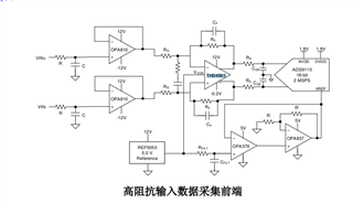
Input signal range: 0 to 10V, single ended signal, frequency 2MHz. The following design is recommended in the user manual. OPA810 input uses 33 Ω+220pf as the filter. Can you help us with the following questions?

1. How to increase the design of overvoltage protection?

2. When the op amp is not powered, what is the state of the device input? If the device input is low resistance, how to prevent the normal input 10V signal from damaging the device;

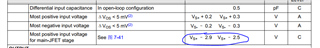
3. If you want to add a clamping diode to point A of the device input in the picture, can you choose the Schottky type? Is the BAT54S of VISHAY OK? The following figure shows some of its parameters.

  • The OPA810 has a protection diodes from the input to the positive supply. A voltage above the supply (when powered off, this is any positive voltage) makes a current flow through this diode. This current must be limited to less than 10 mA, and the supply must be able to sink that current.

    It might be possible to add a series resistor that limits the current. For example, to limit 12 V to less than 10 mA, the resistor must be larger than 1.2 kΩ; larger voltages or smaller currents require an even larger resistor.

    Adding a Schottky diode (with a smaller forward voltage) makes most of the current flow through the external diode. You still have to limit the current if the voltage can become too large.

    Alternatively, add a protection device like the TMUX7462F.

  • Hi Clemens,

    1. With 1k resistor, how much capacitor is used? The input signal is 2MHz, and the cut-off frequency of 33 Ω +220p is 22MHz;

    2. When the power is off, the op amp is in a low resistance state to the power supply and ground. Am I right?

    3. In addition to the current, what other parameters should be considered for the Schottky diode at point A? The diode used here is to consider that the internal diode current of OPA810 is small, and the added Schottky diode can protect OPA810.

    4. Is there a single channel device similar to the TMUX7462F?

    5. Does TI have a DEMO board of my overvoltage protection circuit? I would like to see it.

    Thanks.

  • 1. With 1.2 kΩ, the capcitor should be 6 pF. But that is near the parasitic capacitance of the trace and the opamp input, so you should not add a separate capacitor.

    2. Yes.

    3. With the Schottky diode, the current can be larger, so the resistor can be smaller.

    4. No.

  • Hi Clemens,

    1. Can you recommend an operational amplifier? The input is high resistance when power is off, and the performance parameters are similar to those of OPA810. Because I want to reduce the series resistance of overvoltage protection. I'm worried that there will be other problems with the low pass filter due to the high resistance and small capacitance. I don't see this method.

    2. Does OPA810 bandwidth meet the requirements of 2MHz, 0~10V signal buffer? The bandwidth in AUXILIARY CMOS INPUT STAGE in the manual is 27MHz, which is somewhat confusing.

    3.The positive power supply of the device is different from the negative power supply. Is there a problem? I plan to use+10V, - 5V power supply.

    4. How to understand the most positive input voltage for main JFET stage? Because the power rail increases to 2.9V and 2.5V under this condition.

    Thanks.

  • 1. The search function does not have information about overvoltage-tolerant opamps. I know of the TL072/TL082 (without H suffix), but it's rather slow.

    2. The OPA810 has JFET inputs for most of the input voltages, and CMOS inputs for input voltages within 2.5 V of the positive supply.

    3. What voltage you choose to call "ground" does not matter; the OPA810 sees a 15 V supply.

  • Hi Clemens,

    Maybe I didn't describe the problem clearly, so I didn't understand some of the problems. There are also the following questions.

    1. What is the minimum power supply of OPA810 at 0~10V? The chip in the manual is rail to rail, so I understand that the power supply should only exceed 0.3V. Why is the Most positive input voltage for main JFET stage 2.9V and 2.5V in the manual.

    2. Can OPA810 be used as a buffer for 2MHz/0~10V signals when acting as a voltage follower for opa?

    3. Is the high input impedance characteristic of TL072 in the manual or the result of your actual test? Where is it described in the manual?


  • 1. The OPA810 is a rail-to-rail opamp. With a 10 V supply, voltages up to 7.5 V are handled by the JFET stage, while voltages above 7.5 V are handled by the aux stage. (The transition is visible in figure 7-41.)

    2. Yes.

    3. The TL072's absolute maximum ratings allow input voltages above the positive supply.

  • Is JFET stage only for positive power supply? For example, when the input signal is 0~5V, the power supply should be at least -0.3V and+7.9V. When the input signal is 0~10V, the power supply should be at least -0.3V and+12.9V. Do I understand correctly?

  • No. When you have a 0…10 V signal, the power supply should be (at least) 0 V and 10 V.

  • I don't agree with you.

    Even if the op amp is of rail to rail type, the input and output cannot reach the power supply. The following figure shows the input and output indicators in the manual. Please help explain?

  • The possible output voltage range depends on the load (see figure 7-14). Depending on what is connected to the output, the supplies should indeed a little bit wider. (But not by 2.9 V, unless you want to avoid the aux stage.)

  • Thank you for your patient reply. I have many questions because it is the first time to use this type of op amp.

    1.In the manual, I can't find the specific bandwidth value of G=1 and Vo=10Vpp? How do I calculate this data? The manual gives the bandwidth of G=2 and Vo=2Vpp.

    2.What is the relationship between the recommended operational amplifier bandwidth and signal bandwidth? For example, if the signal is 2MHz, how much bandwidth should the op amp choose?

    3. What is the relationship between the recommended operational amplifier slewing rate and the actual slewing rate? For example, if the signal is 20V/us, what is the slew rate of the op amp?

  • Hello Rengui,

    Please see my answers below:

    1. The gain bandwidth product (GBWP) = Gain * BW for an amplifier.  For the image you shared, the GBWP is 70MHz, and for a G(ain) = 2, the BW is 36MHz.  36 * 2 = 70MHz.  So, for your gain of 1V/V, your BW is 70MHz.  However, as this next point will address, a large-signal output will decrease your available bandwidth.  

    2. Please take a look at the included curves/graphs in section 7.10 of the OPA810 datasheet for 5V supply (curves also available for 10V supply, 24V supply, and variable supply range).  Now, if you actually want a 10Vpp output, you will need a larger supply, such as seen in Figure 7.21.  The larger your output signal, the less BW you have to work with without attenuation of your signal.  The 0.1dB flatness specification is based on this requirement for a flat gain response up to where the response attenuates greater than 0.1dB.  Please use the curves present in the datasheet to assist with evaluating your required supply voltage and gain requirements.

    3. If your signal has a rate of change at 20V/us, you merely need to find an amplifier which can slew at greater than 20V/us.  For example, the OPA810 has a slew rate which varies based on supply voltage and signal swing.  At 5V supply, the SR = 134V/us; at 24V supply SR = ~230-250V/us depending on the signal swing.  All of these values are in excess of 20V/us, your proposed signal requirement.

    Please take some time to review the amplifier datasheets and assess your knowledge of the included specifications.  I have attached this document as a resource: Op-Amp Specs Explained

    Best,

    Alec