This thread has been locked.

If you have a related question, please click the "Ask a related question" button in the top right corner. The newly created question will be automatically linked to this question.

INA851: Are XINA851RGTR fully functional?

Part Number: INA851

Hi,

We bought 40 XINA851RGTR 2 month ago and we have trouble to work with. Therefore I have several questions  :

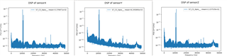
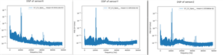
-Are the performances announced in the data-sheet reachable : “Input stage noise: 3.2 nV/√Hz, 0.8 pA/√Hz” for a 1000 gain ?

-Does dual supply generate less input noise than single supply ?

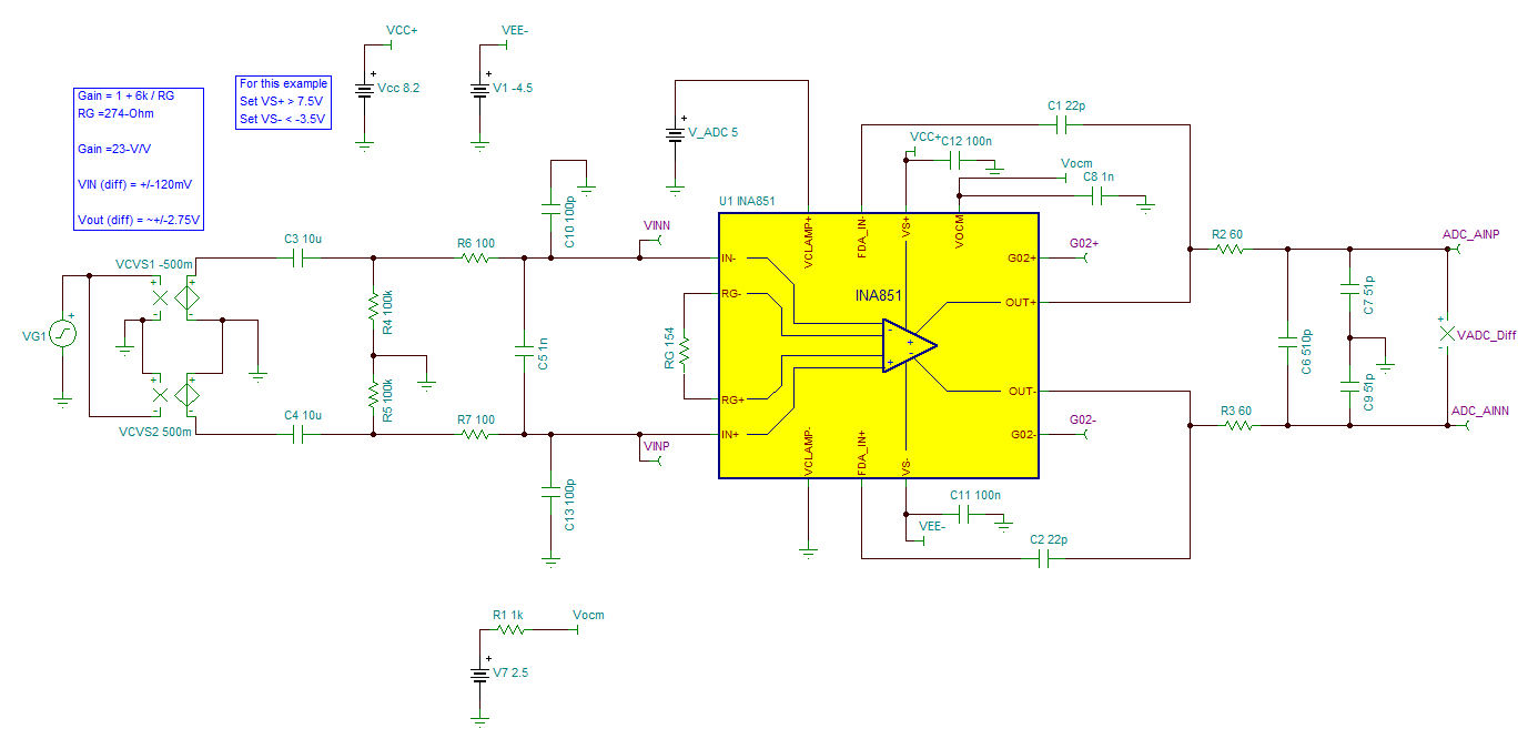
-Are pins FDA_IN+ and FDA_IN- internally connected ? In the datasheet of March 2022 it is written that “pin is internally non-connected on preliminary samples, but will have full functionality in the final device release.”

-Does XINA851RGTR have a precise welding procedure ? Because 1 out of 3 chip seems to not work properly after soldering.

-Does the new version of the INA851 fix issues of XINA851RGTR ?

If you have the answers I will be very grateful

Best Regards,

Maximilien

  • Hi Maximilien,

    please explain what trouble you have.

    Kai

  • HI Maximilien,

     The XINA851RGT early prototype samples/pre-production material did not bond out the FDA_IN- and FDA_IN+ pins. As you have mentioned, the early pre-production advance information datasheet showed that these pins were not bonded out on the early prototypes.

     The connection of the FDA_IN- and FDA_IN+ is an added feature, and its optional.  This option was added flexibility, allows circuit designers to add external feedback capacitors in parallel with the output stage internal feedback to reduce bandwidth (or noise filtering flexibility), similar as you would do on a discrete fully-differential amplifier (FDA).  This feature adds flexibility on certain high-resolution (>16Bit or more) SAR ADC applications where most SARs do not incorporate a digital filter.  

    The XINA851 prototypes pre-release samples of the XINA851RGTR are tested devices, the same input referred noise and expected performance; a number of our Customers sampled the prototypes successfully in their application.  The INA851RGT device was released to production at the end of October,  the samples/inventory available now bond out the FDA_IN- and FDA_IN+ pins.

    Nevertheless, the package type of the pre-production device is the same as the released device, no issues are expected while soldering the device. There are no issues expected on the pre-production device.

     As Kai has mentioned, please share the schematic showing the device connections and explain the soldering issue you are experiencing.

    Thank you and Regards.

    Luis


  • Hi Maximilien,

    Also, just in case this is not related to a soldering issue, please show the schematic showing the supply connections in the system: VS+ , VS- , VCLAMP+, VCLAMP- , as well as the VOCM voltage. 

    Let me know the expected max input signal differential voltage range VDIF= (IN+) - (IN-); input signal common-mode voltage range: VCM =  {(IN+) - (IN-)} / 2 (where common-mode voltage is the average voltage in the signals); and output voltage range in the application to verify the instrumentation amplifier operates within its linear range.

    Kindly elaborate about the issue, and describe the performance issue seen between the working and not working devices.

    Thank you and Regards,

    Luis 

  • Hi Kai and Luis

    Thank you for the quick response and sorry for my late reply it was public holiday last Friday. As you asked, you will find a schematic of the INA851’s connections.

    Thank you for confirming that FDA_IN’s pins are disconnected, we have already order the release version of INA851 to test it.

    We are not sure of the source of our problems. On our PCB, we use 6 INA851 that work together with 4 CS5381 as ADC. Theses components are divided in two groups, one for each sensor. A sensor is based of 3 wired coil, each coil have an equivalent resistance of 50 Ohm and link to one amplifier X, Y or Z. You can see how a group of components looks like in simplified_schematic_sensor.pdf. We collect the data from the ADC and with an homemade software we draw a DSP for each amplifier, 1 DSP of 3 has a noise floor not flat unlike the others. We have the same wrong DSP for our 2 sensors but not for the same channels. For the first sensor it is Y, for the second is X. That is why we think our problems are due to amplifiers.

    Also, we are not sure about the input bias we have implemented, could you please share your schematic of the INA851’s entries.

    For supply connections in the system :

    • VS+ = 8,2 V
    • VS- = GND

    We think to pass to dual supply if it provides us a better SNR and CMR.

    • VCLAMP+ = 5 V max input supported by the ADC
    • VCLAMP- = GND
    • VOCM = 2,5 V it is fixed by our ADC CS5381
    • VDIF= 120 mV
    • VCM = 40 mV
    • OUT+ and OUT- are correctly centered to the voltage fixed by VOCM, 2,5V.

    Best regards,

    Maximilien

    INA851_schematic.pdfsimplified_schematic_sensor.pdf

  • Hi Maximilien,

    Thank you very much for the detailed information.

    The INA851 is similar to standard instrumentation amplifiers, the main difference is that incorporates a fully-differential amplifier output.  Each amplifier inside the INA has it’s own input and output swing limitations.   These limitations combine into an overall input differential and common mode voltage versus output swing range limitation. This relationship can be complex and generally cannot be determined with a simple equation or data sheet parameter.  We offer an excel calculator to verify the device is inside the input/output linear range.  More information on this tool at the bottom of this post.

    You are correct, that using bipolar supplies will provide more freedom on the input common-mode range. The schematic shows the sensor AC coupled to the inputs of the INA851, with 1μF capacitors, and then 100k resistors connected to a DC bias voltage of +5V.  If you plan to use bipolar supplies; I would recommend to connect the 100k resistors close to the mid point of the VS+/VS- supplies, but there is some level of flexibility here as long there is a voltage headroom to the VS+/VS- supplies.

    The output voltage swing requires a minimum 1.4V headroom from the VS+/VS- supplies, and when using the clamps, the clamp pins must be at least 1.5V from the VS+/VS- supplies.   

    For example, assuming the max. input differential signal (from the sensor) is ±120mV, and looking at CS5381 fully-differential full-scale range, 1.07*VA = 5.52Vpp, or essentially, ±2.76-V differential voltage, you could set RG=274Ω, for a front-end gain of 1+6k/274 = 23-V/V.

    In this case, setting the circuit, with the 100k resistors assumed to be connected to GND (setting input common-mode to 0V), with supplies V+= +8.2V (or at least V+ >+7.5V), V- = -5V (or more negative than V- < -3.5V), VCLAMP=+5V, VCLAMP=GND, VOCM=+2.5V provides headroom:

    Edit, 11-16-22, corrected figure below, with suggested low-pass filter at the input sof the INA851 to filter extrinsic noise:

    The CS5381 is a delta-sigma ADC, it samples the input at 6.144MHz, and it is best to use C0G/NPO grade capacitors for low-distortion results on the R-C-R filter between the INA851 output and ADC inputs, as well as any other low-pass filters in the signal path. 

    The R-C-R filter at the ADC inputs plays a role in the performance.  One purpose of the filter is a charge reservoir to filter the sampled input of the ADC. The charge reservoir reduces the instantaneous charge demand of the amplifier, maintaining low distortion and low gain error that otherwise can degrade because of incomplete amplifier settling. On our side, the INA851 has provided good results using an R-C-R filter with 60.4Ω-510pF-60.4Ω; and 51pF common-mode capacitors at the output driving other delta-sigma ADCs, providing low noise results.  The FDA_IN+/FDA_IN- 22-pF capacitors shown above are optional.  

    Regarding the INA851 Input voltage range Calculator (excel) tool:

    You can download the excel tool on the link below and verify the amplifier is in range:

    INA851 Input-Output Range Design Calculator

    The tool consists of two sheets:

    On the first sheet, “INA851_Vin_Vout_tool”:

    The User fills the highlighted cells in blue with required voltages: VS+, VS-, Front-End Gain, Back-End Gain, Input differential voltage, input common-mode Voltage, VOCM voltage, VCLAMP+ and VCLAMP- (if Clamps Enabled). The Excel provides resulting VOUT+, VOUT-, and VOUT differential voltages.  The tool highlights in red any voltage out of range, and displays warnings in red if the device is outside of linear range.

    Similarly, the second sheet,  the tool provides an Operating Range Chart provides with the valid input & output ranges for this Instrumentation Amplifier. Use VICM to scroll bar to adjust the input common mode.

    Attached is a pdf document with detailed instructions:

    INA851 Input and Output Range Design Calculator Instructions.pdf

    Thank you and Regards,

    Luis 

  • Hi Maximilien,

    When using the +/- VS bipolar supplies, please ensure to connect the thermal pad to the most negative supply, VS-.

    Thank you and Regards,

    Luis

  • HI Maximilien,

    On the suggested circuit, I placed a low-pass filter at the input of the instrumentation amplifier to help reduce high-frequency extrinsic noise,  using100-Ω-1nF-100-Ω, differential filter, and 100pF common-mode capacitors, where the differential capacitor is 10x larger than the common-mode capacitors. You can of course adjust the corner frequency of this filter or modify the circuit per the application requirements.

    Thank you and Regards,

    Luis 

  • Hi Luis

    Thank for you feedback and the INA851 calculator, we are currently studying how we will implement this on our PCB.

    I will keep you updated, best regards

    Maximilien

  • Thank you Maximilien,

    I will also reach out via direct email to provide my contact information, in case you need anything.

    Kind Regards,

    Luis