This thread has been locked.

If you have a related question, please click the "Ask a related question" button in the top right corner. The newly created question will be automatically linked to this question.

LMH6601: Request for schematic review

Part Number: LMH6601
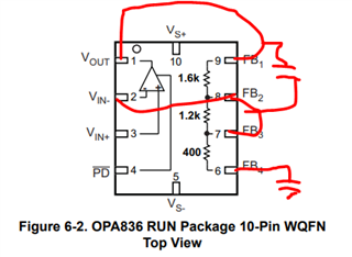
Other Parts Discussed in Thread: LM7705, THS4211, OPA836, OPA838, OPA830

Hello,

Could we have our schematic reviewed?

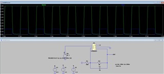
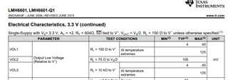
The LMH6601 circuit is on Sheet 17.

The requirements are

  • Square wave with adjustable amplitude between 1.5V and 2.5V
    • My approach is to control the amplitude with the DAC
  • Frequency would be between 0.1 and 2 MHz
    • The edges need to be sharp
    • I think this means we need to retain all the harmonics

Thanks for support

Andrew

FIBERSENSE_V1P16.pdf

  • Hi Andrew, 

    After looking over page 17 of the schematic for the LMH6601, I did have a couple suggestions and some clarifying questions on your design.

    My first comment is that the SD pin in the schematic is grounded which disables the amplifier. This pin's voltage should be between 2.97V - 3.3V for proper enabling of the device. This is also highlighted in the typical characteristics tables for the 3.3V section. 

    I did have a question regarding the expected input to the LMH6601. The requirement is a 2.5V square wave output on 3.3V to ground supplies. I am curious what is your input and if you plan on having any sort of DC offset in order to be within the linear input range of the amplifier. For this 2.5V square wave output, there will likely have to be an offset, so the output voltage range is also within its linear range. Just some things to consider for this design since you are using a single supply configuration.

    As far as the design goes you should have no issue with the capacitor and choice of resistors. Although a quick suggestion would be to include decoupling capacitors at the supply pins near the device. I do see you have some throughout the schematic, but it helps to include some near the supply pins of the amplifier. During layout the goal is to have them as close to the pins as possible.

    Best Regards,

    Ignacio

  • Hi Ignacio,

    The SD pin has been updated, tied to 3.3V via 10k resistor.

    Below is my simulation.  The output from the DAC (THS5641) is a square wave between 0V and 0.6V, which gets amplified by LMH6601.

    I've updated the feedback resistor so at the max DAC output the LMH6601 can reach ~3V, to give a bit of a head room above 2.5V.

    A decoupling capacitor of 0.1uF has been added to the supply voltage.

    It may be important to make the rising edge of the square wave sharp.  I think the bipolar supply voltages may help in case.  Is this a valid assumption?

    In terms of an offset, I believe THS5641 can generate a square wave from 0 to 0.6V.  Otherwise I may need to use the differential outputs.

    Thanks for your support

    Andrew

    FIBERSENSE_V1P17_pg17.pdf

  • Hi Andrew,

    keep in mind that the "large signal open loop gain" of LMH6601 is specified for "0.3 V < VOUT < 3 V". This means that you leave the linear operating range when your output signal falls below 0.3V.

    One remedy is to use a negative supply voltage of < -0.3V.

    By the way, I think the output needs to be loaded symmetrically. You would need an additional 50R dummy resistor from "IOUT2" to signal ground. Also keep in mind that the best performance will be achieved when using both outputs (differential signalling) as discussed in the datasheet of DAC.

    Kai

  • Well Andrew, Kai is right - you really cannot swing to ground on the RRO parts without sticking there a bit, Also - why do you have that 600 ohm in series with the supply line - I see now, that is a ferrite bead. The LM7705 was done for this purpose, to provide a bit of output headroom by supplying a -0.23V on the negative rail. That overdrive into to ground may not be simulating that well in the model. 

  • Hi Kai and Michael,

    Thanks for your inputs.

    • Updated the op amp to THS4211, just to make certain of the wide bandwidth so the rising edges will be sharp
    • Added LM7705 for the negative supply
    • Added 49.9R to IOUT2

    Please let me know of any issues.

    Regards,

    Andrew

    fibersense_v1p17.pdf

  • Andrew, you probably should not be switching to a non-RR out device like the THS4211, here are your choices in RRout, higher slew rate VFA devices from TI or NSM, Be careful with those SSBW for the CMOS parts - those are false high numbers not even remotely related to the true GBP. The OPA830 is the highest slew rate, this table was resorted by ascending slew rate, and actually the OPA836 is the much newer part, looks pretty good at much lower quiescent power - keep in mind your gain of 5 will be operating these parts are relatively low SSBW - say for the OPA836, which has a true GBP of 130MHz in the TINA model, that will be a SSBW of only 26MHz. You might want to RC filter your DAC edge into the V+ input to say about 50MHz since its sharp edge will not get through anyway - The OPA838 could do better but might be a little ringy at that low of a gain. Also, a 2.5V step with 26MHz BW will not be asking for much slew rate anyway - no more than 200V/usec. All of this would show up in simulations if you ran those. 

    Sorted VFA RRout.xlsx

  • Hi Michael,

    Thanks again for your feedback.

    I've decided to go with OPA836.  I wanted to use SOT-23 but not available.  

    So I'm using the QFN-10 part.  I have left the FB pins unconnected.

    The simulation seems to show a sharp edge but couldn't really quantify.

    Please review.

    Regards,

    Andrew

    fibersense_v1p18_pg17.pdf

  • Looks good to me, bummer the SOT23-6 is out of stock?

  • And you could get your gain of 5 using the internal R's, like this, short the 1.2kohm out and use the 400 for the gain element and the 1.6kohm for the feedback element. 

  • Hi Michael,

    Thanks for your response again.

    I think for now I would stay with external gain resistors so I can try different values on prototypes.

    Later when the values are fixed, I can try to use the on-chip resistors.

    Thank you so much for your support.

    I'll keep you posted on testing.

    Regards,

    Andrew