This thread has been locked.

If you have a related question, please click the "Ask a related question" button in the top right corner. The newly created question will be automatically linked to this question.

TLV1805: why is the different output V of TLV1805 between simulation(Pspice) and measurment ?

Part Number: TLV1805

hi team

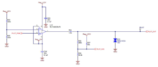
my applicaiton is AC charging pile that refer to TIDA-010071 document . so using TLV1805 for Control Pilot Signal is our solution.

my question is 

  1. why is the different output(PIN1) V of TLV1805  between simulation and measurment if pin3 and pin 4 is 0V .    the output V of simulation is 12V ,but actual measurement is +12 to -12 4KHz wavefrom 
  2.    
  3. what is a correct status 
  4. which a parameter of TLV1805 cause this problem such as Vos........

thanks 

  • Hi Ethan,

    Thanks for reaching out. When you connect both inputs to 0V, there is always going to be some level of variation, noise, and offset so you're going to see different results between part to part. This can cause the chatter that you see in the output. We recommend tying input to GND and the other input to a known voltage source such as VCC.

    -Chi

  • hi Chi

    thank your reply 

    both (pin3 and pin4)=0V  mean 3.3V does not supply pin3 and pin4 is set to low from MCU  so it is not actual 0V(GND) 

    and one more thing is how much noise will be triggered and output voltage by OP specifications.is it  VIO or Vhys?

  • Hi Ethan,

    I am not sure what you mean by your question. There is noise coming from your inputs as well as internally from the comparator, but it is not something we have in the specs. VIO (offset) is how much the IN+ is shifted from the IN-. VHYS is how much internal hysteresis the comparator has, meaning it has the 14mV of separation so that it can protect against chatter if the expected noise is smaller than 14 mV. Please see this video for more in depth review of the VOS and VHYS An Overview on Comparators - YouTube. I highly recommend setting the inputs to separate voltage levels as you do not want the input to trigger upon its own wideband noise, causing chatter. 

  • Hello Ethan,

    As Chi explained, both inputs at 0V is technically an invalid condition. The output is indeterminate when IN+ = IN-. Actual output will be determined by the individual devices offset voltage. DO NOT rely on the trend of offset voltage to set the output.

    Can you run the divider off of the comparator +12V instead? With appropriate changes to R53, of course. That way if the 3V3 controller voltage is off, the negative input is still biased at 1.65V, which will provide the correct output when the controller is off.

  • thanks  the video is useful for me 

  • ok   i will  try it