This thread has been locked.

If you have a related question, please click the "Ask a related question" button in the top right corner. The newly created question will be automatically linked to this question.

OPA593EVM: Output oscillation with default configuration

Part Number: OPA593EVM
Other Parts Discussed in Thread: OPA593, LM317

Dear Technical Support Team,

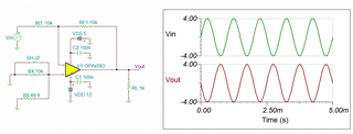
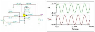
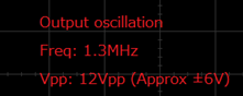
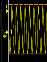
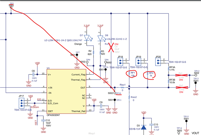
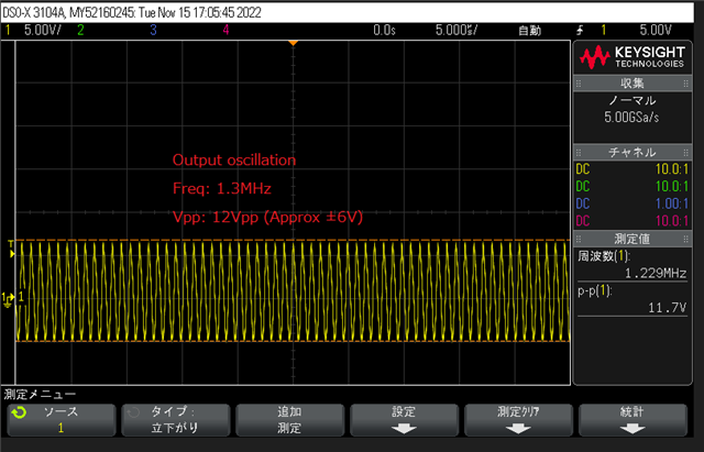
Output of OPA593EVM is Oscillating with default configuration when suppling the dual voltage(12V、-5V).

User guide page16(4.1.1 EVM Default Configuration) said that "The OPA593EVM ships in a configuration that allows the EVM to be directly applied as an inverting or noninverting amplifier" 

It causes both 10kΩ(JP18) and 1kΩ(JP19), however no feedback resistance helps output stable by bypassing FB resistance(Connecting TP10(AMP OUT) to (TP3 AMP IN))

Any jumper setting  and some input(AC or DC signals ) doesn't stop it.

Could you check the same situation with your OPA593EVM on lab?

Best Regards,

ttd

  • Hi TTF,

    are we referring to the schematic of figure 4-2 of EVM? What jumpers exactly are set?

    And why do you want to make a short circuit connection from the -input to the output of OPAmp?

    Have you inserted an isolation resistor when probing the output? What else is connected to the output apart from the probe?

    Kai

  • Hi ttd-san,

    User guide page16(4.1.1 EVM Default Configuration) said that "The OPA593EVM ships in a configuration that allows the EVM to be directly applied as an inverting or noninverting amplifier" 

    Could you translate the OPA593's EVM configurations on paper via the simulation? The EVM is fairly busy configurations that are trying to cover the multiple op amp driving circuits.  

    BTW, the EVM has been tested, verified and validated extensively,  and we did not find any oscillation issues with OPA593 or the EVM. 

    For inverting configuration, the default setup in Figure 4-2 should be configured as fellows approximately.  

    OPA593 EVM Inverting Config 11182022.TSC

    For Non-inverting configuration, the default setup in Figure 4-2 should be similar to the schematic as follows. 

    OPA593 EVM Non-inverting Config 11182022.TSC

    You mentioned that the setup is using dual supply voltage, -5Vdc and +12Vdc, but the scope is shown the oscillation with ±6Vpk or 12Vpp centered around the GND. Could you check with your setup? Also, please let us know what is the  applied load in your evaluation. 

    Best,

    Raymond


  • Hello ttd,

    I designed the OPA593EVM and have used it many times in various gain including as a unity-gain (+1 V/V) buffer amplifier. I haven't ever seen the OPA593 oscillate unless I have intentionally added a large capacitive load that reduces the phase margin to the point where oscillation occurs.

    I have one set up in the lab as a unity-gain buffer amplifier. On that board the 10 k, RF1 has been replaced with a 0-Ohm resistor replacement. I have the OPA593 non-inverting input terminated to ground with a 50-Ohm line terminator. I ran a couple of tests with various symmetrical and asymmetrical power supply voltages including +12 V/-5 V to see if I could get the OPA593 to oscillate. I left the non-inverting input terminated and observed the output and no oscillation occurred. Then I drove the buffer amplifier with a 1 kHz source of various levels and that didn't bring about any oscillation. Nothing I tried resulted in oscillation including leaving the output unloaded and loading it with various resistive loads. This is just as I have always found the OPA593 to behave.

    If the OPA593 is to oscillate due to an excessive capacitive load the frequency of oscillation should be near its unity-gain bandwidth frequency of 10 MHz and the amplitude be low in level. The oscillation you show is a large-signal (12 Vpp) and a frequency of 1.3 MHz. That doesn't quite fit anything I would expect for the OPA593. I am wondering if the OPA593 has been damaged in some manner and the oscillation is an odd, unexpected result?

    Regards, Thomas

    Precision Amplifiers Applications Engineering

  • Hi Raymond,

    Thank you for your reply and simulation.

    I apology that ±6V might not be correct. GND is not center such as -5V and 7V because of -5Vdc and +12Vdc you mentioned.

    R21(1kΩ load) doesn't stop oscillation either with or without and then output connector is connected only oscilloscope.

    This oscillation occurred with ±12V dual supply.

    Best Regards,

    ttd

  • Hi Thomas,

    Thank you for your reply.

    I understand that your  EVM doesn't oscillate any configuration except for high cap load.

    I purchased additional OPA593EVM. I will check it.

    Best Regards,

    ttd 

  • Hi ttd-san,

    Thomas is out of office. 

    OPA593 will oscillate when it is driving a larger capacitive load. The op amp instability is resulted from the additional pole generated within a feedback loop between OPA593's Zout and capacitive load. If driving capacitive load is required for the application, we have to find a way to compensate the feedback loop.  Please specify the capacitive load for the driving requirements and perhaps we can stabilize the circuit and configuration.  

    For the op amp compensation techniques, please check out the video link below. There are 7 video clips about the op amp stability topics in this series. 

    https://training.ti.com/ti-precision-labs-op-amps-stability-capacitive-loads?context=1139747-1139745-14685-1138805-13952

    If you have additional questions, please let us know. 

    Best,

    Raymond

  • Hi Raymond,

    Thank you for your reply.

    In my case, output capacitive load is up to 220uF, so compensation techniques you suggested should be used.

    By the way, datasheet is still "Preview" and output capacitance is TBD.

    When does the datasheet become "Active"?  

    Best Regards,

    ttd

  • Hello ttd,

    A 220 uF capacitance is a huge capacitive load for an op amp. I will look into compensating the OPA593 buffer amplifier with that C-load, but be aware that even if there is a suitable solution its highly likely the circuit's ac bandwidth will be very low. 

    Before I spend the time developing a compensation scheme, what is the acceptable minimum -3 dB bandwidth needed for your application? Can the application tolerate the voltage drop of an added  series resistance (Riso) connected after the OPA593 output/ feedback connection point and the C-load?

    Regards, Thomas

    Precision Amplifiers Applications Engineering

  • Hi TTD,

    By the way, datasheet is still "Preview" and output capacitance is TBD.

    A tolerable output capacitance would be something in the 100pF range but not 220µF. No amplifier will tolerate a 220µF capacitance being directly connected from the output to signal ground, because this means a short-circuit at higher frequencies. 220µF gives an impedance of 0.07Ohm at 10kHz...

    Please explain why you want to mount such a high load capacitance.

    Kai

  • Hi Thomas,

    Thank you for your reply.

    Usually OPA593 is configured for buffer(1V/V) and input and output are DC voltage such as 5V like power supply IC.

    However I need to consider steep load change from 0mA to 200mA.

    When I consider this about 1us (actually several us) with margin,  minimum -3 dB bandwidth  is 350kHz(1us = 0.35 / freq).

    https://e2e.ti.com/support/amplifiers-group/amplifiers/f/amplifiers-forum/1171071/opa593-unexpected-pulse-during-steep-load-change

    Best Reagrds,

    ttd

  • Hi TTD,

    Usually OPA593 is configured for buffer(1V/V) and input and output are DC voltage such as 5V like power supply IC.

    So what you need is a voltage regulator? Then I would strongly recommend to take a voltage regulator chip like the LM317. Voltage regulator chips are designed to operate stably with lots of capacitve load and to allow steep load changes. The LM317 can easily programmed to any output voltage by applying a control voltage to the ADJ-pin. I'm pretty much sure that the LM317 will behave better in your applicaion than the OPA593.

    Kai

  • Like it's done in the STK500 board, e.g.:

    Here the output voltage of LM317 is programmed by a PWM signal coming from the left.

    Of course, the circuit may need to be optimized for your application.

    Kai

  • Hi ttd,

    I agree with Kai that your application can be better served by a voltage regulator circuit. Note that the circuit provided by Kai only sources current to a load. 

    I am concerned about the 1 us current step change response at the output; especially, with the 220 uF load capacitance. If that is truly the requirement I am not sure we can provide a solution.

    Regards, Thomas

  • Hi Thomas and kai,

    Thank you for your reply and  suggesting a voltage regulator circuit.

    OPA593 has current limit and I need to use it. 
    Input DC voltage is changed  sometimes such as 5Vdc and 3.3Vdc and negative voltage(-2Vdc) etc.. from DAC.

    I believe that this is the merit to use OPA593.

    1us current step(actually under 10us) and 220uF(or 100uF) is currently targeted value.

    If you consider max output capacitance and current step, could you share it? 

    >Can the application tolerate the voltage drop of an added  series resistance (Riso) connected after the OPA593 output/ feedback connection point and the C-load?

    ⇒Riso is following figure you described on APP note might be ok.

    www.ti.com/.../sboa553.pdf

    My circuit have feedback path to compensate IR drop by sensing load, so I supposed that it cancels Riso voltage drop, too.

    Best Regards,

    ttd

  • Hi ttd-san,

    Could you tell us what is the circuit's actual application? We can recommend something else if we know the application. 

    Regarding to step response ~1usec, OPA593 has a slew rate of 40V/usec. If it is driving a pure resistive load, delta 5V voltage rise will take 5V/4V/usec = 1.25usec. Since the current follows the voltage in the configuration, the current step rising and falling time will also take 1.25usc. With the capacitive load, the RC time constant will not meet your design requirements.  

    ⇒Riso is following figure you described on APP note might be ok.

    Kai mentioned that 220uf at 10kHz is equivalent to 1/sC = 1/(2*pi*10kHz*220uf) = 72mΩ load. 100uf capacitor is equivalent to 159mΩ impedance load at 10kHz. I need more information about the application before I am able to comment on the Riso circuit. 

    Riso compensation works adequate well for low output current application. For high current application, Riso of 5V/200mA = 25Ω is already shown 5V of voltage drop across the compensation, which it may not feasible for the application. Again, we need to know what you are trying to do. 

    Best,

    Raymond 

  • Hi ttd-san,

    I am going to close this inquiry, since I moved the support forum internally. 

    If you have additional questions, please let us know.

    Best,

    Raymond