This thread has been locked.

If you have a related question, please click the "Ask a related question" button in the top right corner. The newly created question will be automatically linked to this question.

INA231: help review the schematic of INA231AIYFFT

Part Number: INA231

Hi team,

Can you help review the schematic of INA231AIYFFT and PCB layout in the attachment?

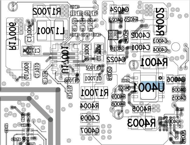
INA231AIYFFT.xlsxGourami_MB_PCB_V1_20221125_1534(2).pdfGourami_MB_PCB_V1_20221125_1411.brd

Thanks 

Best regards

Lillian

  • Hello Lillian,

    Sorry for the delay. We were out on national holiday and weekend.

    I am looking this over and will respond shortly.

    Sincerely,

    Peter

  • Hey Lillian,

    I cannot open the .brd file. My Allegro PCB Viewer software is saying the file is corrupted or copied with ASCII and that it should be copied with binary format. A simple screen shot of the INA231 and surrounding circuitry should suffice if that makes it easier.

    As for the schematic everything looks good except that NC1 pin should be floating and not tied to GND.

    Sincerely,

    Peter

  • Hi Peter,

    Thanks for your reply!

    Can you help check the layout by searching the "U4001"in the PDF file? or simple screen shot shown as below? 

    Thanks 

    Best regards

    Lillian Liu

  • Hey Lillian,

    The layout looks fine.

    There are three things I should note about the layout of the 20mOhm shunt resistor. One, the INA231 is not sensing the shunt with proper Kelvin sense connections. There is no separation of Kelvin force and sense connections, they are the same. Usually this is much more important with smaller shunt resistance <=1mOhm because the resistance from the solder can add hundreds of micro-Ohms.

    Second, the INA231 is not sensing directly underneath the pads of the resistor. Thus, it is sensing 20mOhm + the resistance of the copper path + the solder resistance (as mentioned above). The other problem here is that you are not sensing directly under an in the center of the shunt pads, rather they are sensing on the inside edges of the pads. When you or manufacturer measures resistance of this resistor, it is usually at the center of the pad, not at the edge, which could change the effective sense resistance.

    Lastly, the orientation of the shunt resistor and the orientation of the current density field lines (blue vectors) is not well matched up. This can result in a gain error where most of the current flows through a portion of the shunt resistor as opposed to being evenly distributed across area of the shunt resistor. 

    Sincerely,

    Peter