This thread has been locked.

If you have a related question, please click the "Ask a related question" button in the top right corner. The newly created question will be automatically linked to this question.

INA333: Analog Engineer's Calculator VOUT max and VOUT min calculations

Part Number: INA333

Hello,

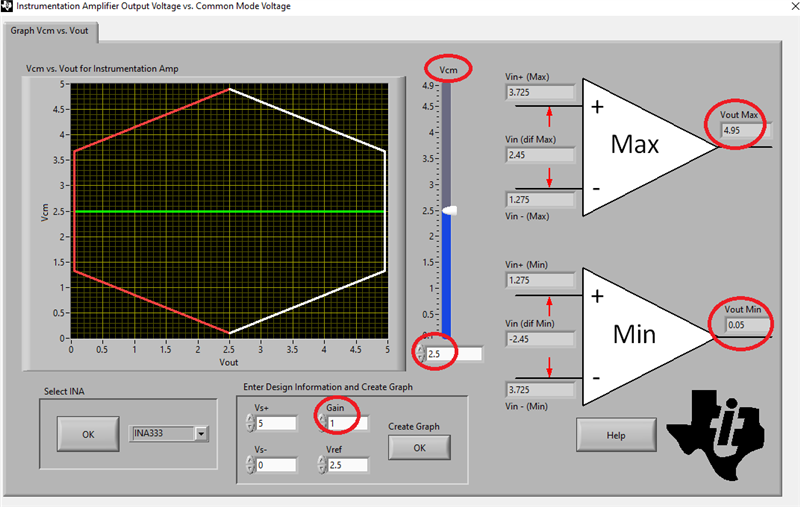
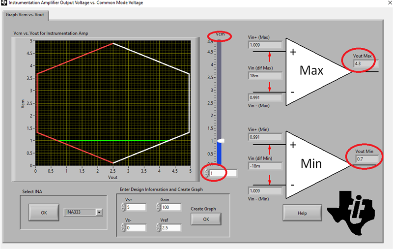
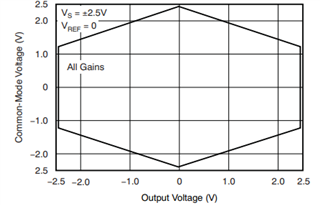
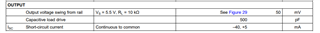
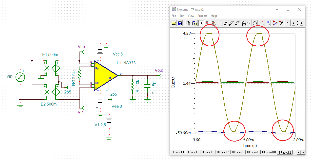
I am looking at the Analog Engineer's Calculator with my customer on the INA Vcm vs Vout tab for the INA333 as the selected component. The outputs are limited to 4.7V max and - 0.3V min with 5V V+ and 0V V- with a 2.5V reference. But when I look at the datasheet it says the output is:

Am I missing something?  

John

  • John,

    The INA333 datasheet shows the best case input and output voltage ranges based on the INA333 internal circuit topology.  However, these ranges may be further limited depending on the specifics of the application like supply voltage, reference voltage as well as gain and Vcm - see below.  This is the main reason why we have INA Vout vs Vcm calculator - to show the input / output voltage range variations for different configurations used.

  • Hi Marek,

    Is it safe to assume that the device could do better than the calculator shows for light loads? I am looking at Figure 29. My customer's application is INA333, Vs- 0V, Vs+ 5.0V, gain 50V/V, Vref 2.5V, and common mode 2.507V. When I apply these parameters in the calculator, I get 0.3V to 4.7V. I am waiting to hear back what the output is loaded with. 

    Thanks,

    John

  • Hi John,

    Marek is out for the next few days so I'll try to address; in general, yes, your statement is true.  The output swing should only be limited by the output amplifier's ability to swing to the rail in the configuration you have mentioned above.  Figure 20 appears to support this (assuming all voltages in your plot are shifted down by 2.5V): 

    It looks like the output limitation goes to almost +/- 2.45 V, which would correspond to the "Output swing from Rail" spec. of 50 mV:

    Note, this would be at room temp., which is presumably where the discrepancy is between the calculator and the data sheet.  

    I'll check and see if there's any more information on why it would be +/- 300 mV from the rail.

    Regards,
    Mike

  • Hi Michael,

    For their application, the output of the INA333 goes into another op amp so the loading is high impedance and therefore very small. I tried running a simulation in PSPICE for TI and am having convergence issues. See attached. Sorry I am traveling and didn't have much time to try and debug. 

    Thanks,

    JohnINA333_Sim.zip

  • Hi John,

    There's a host of problems, several of which seem to be related to the naming and PSPICE for TI (you can't have spaces in any of the file names, this is an issue that is tough to figure out).  On the circuit side, the inputs on your simulation weren't set up correctly - the common-mode was at GND.  You should be able to make the changes shown below:

     I built this in TINA for verification:

    In the TINA sim, the outputs are able to go 70 mV from the positive rail, and 30 mV from the rail on the negative side.

    This aligns with the claw curve showing better output drive on the negative side.  So, overall, the performance to the rail should be better than 300 mV as shown in the calculator. I'll check to see why the calculator shows 300 mV but this could be a few days.

    Regards,
    Mike

     INA333_John_Example.TSC

  • John,

    I believe the Analog Engineer’s calculator has an error in INA333 model.  Under the above conditions its output should swing within 50mV to either rail at 25C and max 70mV to the rails over the entire temp range.  We’re working on fixing it.

  • Hi John,

    simulating the internal circuitry of INA333 with three ideal OPAmps shows that no internal node of the INA333 seems to go into saturation:

    john_ina333.TSC

    So the INA333 should provide the full output voltage range.

    But keep in mind that the output range specification mentioned in the datasheet

    "Output Range: (V–) +0.05 V to (V+) –0.05 V"

    means the saturation output voltage where the output stage of OPAmp no longer runs in its linear operating range. To operate linearily, on the other hand, the output voltage should stay 100mV away from the supply rails. See the "gain error" and "gain nonlinearity" specifications in the datasheet.

    You can see the saturation effects very easily in Michael's simulation, by the way:

    Kai

  • Thank you both! This is super helpful! Let us know when you get the engineer's calculator updated. 

    John