This thread has been locked.

If you have a related question, please click the "Ask a related question" button in the top right corner. The newly created question will be automatically linked to this question.

LMV321-N-Q1: Output tolerance calculation

Part Number: LMV321-N-Q1
Other Parts Discussed in Thread: AMC1311-Q1, AMC1311, LMV321

Hi TI expert,

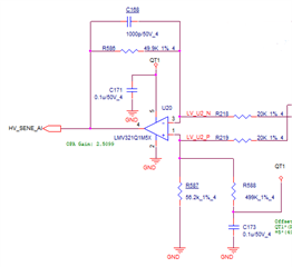
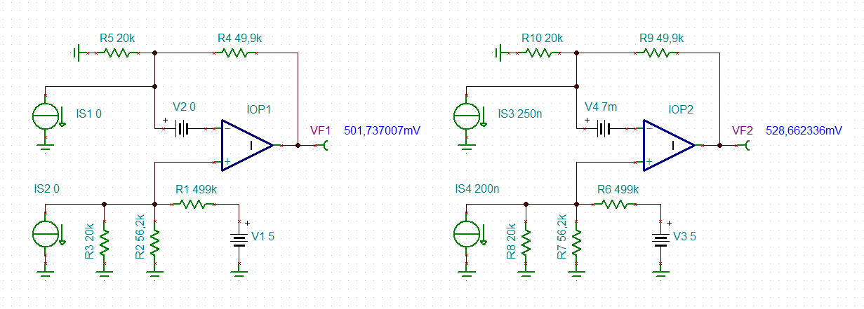
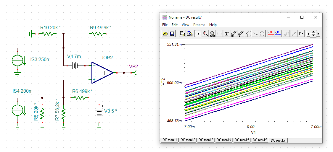
May I know how to judge the Vout tolerance if we short the "right side" of the R218 & R219 together in the below application?
We add a 0.5V offset by R588/C173/R587.
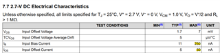
As I know the Ibias and Vos will affect the Vout but not quite sure how to judge the output tolerance based on that.
Could you guide us on how to calculate the VOUT tolerance for this case? we need to do the calibration for cascaded ADC from "HV_SENE_AI".

QT1 = 5V with 1% tolerance.


Looking forward to your reply.
Thank you.

  • Hi Chia,

    take an ideal amplifier and add the input bias currents and input offset voltage externally:

    chia_lmv321.TSC

    You still have to consider the manufacturing tolerances of resistors.

    Kai

  • Here with 1%-toleranced resistors and 1%-toleranced 5V supply voltage:

    chia_lmv321_1.TSC

    Kai

  • Hi Kai,

    Thank you for the data.

    1. The IB shall be the current flow into the IN+ & IN- pin, am I right? Will we see a different result based on above figure?

    2. Although we short the input side together, does that means we should consider it as GND like how you connect those 20k ohm in above figure?

  • Hey Chia,

    The error contribution from input bias current will be the input bias current (Ib) combined with the input offset current (Io). Kai has taken both into account with 200nA for one input and 250nA for the other input.

    From the datasheet, you can see where these numbers came from. 

    Since the device has a bipolar input stage, the max Ib is 250nA and the max Io is 50nA you would subtract the Io from the Ib for the worst case offset. While Io can be either positive or negative, the Ib is specified as 250nA max, so the worst case Io would be 250nA on one input and 200nA on the other. Your worst case error for this would be placing the higher bias current on the input that sees the greatest impedance.

    You can minimize your error from input bias current by impedance matching your inputs. This makes the voltage difference due to your input bias current just the input offset current. The max value for input offset current is 1/5 your input bias current. 

    Best,
    Jerry

  • Hi Chia,

    how do you connect the 20k resistors together during the calibration? Do you disconnect them from the original circuit during the calibration? Are they entirely floating then and only be connected to themselves?

    Can you show a complete schematic explaining the calibration switchings?

    Kai

  • Hi Kai,

    We do not have a plan to actually floating the input side for the testing.

    Just wondering what would it be if we float the right side of those 20k ohms.

    The purpose is to do the calibration for the following ADC. 

    The right side will be AMC1311-Q1's differential output pins.

    But we just assume the AMC1311-Q1 output is zero.

    Thank you. 

  • Hey Chia,

    Do you have any further questions? 

    Please let us know if your issue is resolved.

    Best,
    Jerry

  • Hi Jerry,

    No Further questions so far.

    Thank you for your help.

  • Hi Chia,

    But we just assume the AMC1311-Q1 output is zero.

    Hhm, I don't think that you can assume this, even not if the AMC1311 is powered down. The input bias currents of LMV321 will unwantedly bias pn-junctions within the powered-down AMC1311 resulting in potentials at the output of AMC1311 differing from zero Volts.

    Kai