


Other Parts Discussed in Thread: TINA-TI
Hello,
I need to drive a 10uF capacitve load which acts as a low pass filter to block the dc current.
The OPA452 amplifies the voltage of a rectangular signal and 2 transistors in a push pull configuration amplify the current. The circuit is also stated in the datasheet on page 12: https://www.ti.com/lit/ds/symlink/opa452.pdf?ts=1674827094813&ref_url=https%253A%252F%252Fwww.ti.com%252Fproduct%252FOPA452
I chose a value for the capacitor Cf so that there are no interefrences in the voltage when driving a light load with high currents. But if the load is for example 30kOhms you can still measure peaks in the Signal. If I increase the value for Cf the signal is not rectangular anymore and gets more round as the high frequencies are not amplified enough anymore.
Here is a picture of the problem: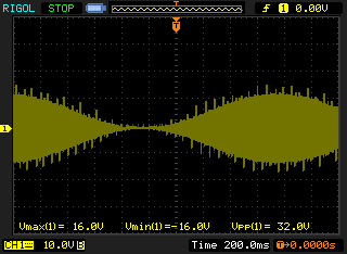
What can I do to compensate that better and still having a rectangular looking signal?
I hope somebody can help me.

