This thread has been locked.

If you have a related question, please click the "Ask a related question" button in the top right corner. The newly created question will be automatically linked to this question.

PGA309: Register configuration and EERPOM

Part Number: PGA309
Other Parts Discussed in Thread: XTR115

Hello

I encountered the following problems when using PGA309. I do not know the reason, please help.

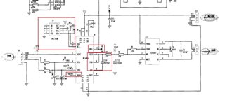
1.In the absence of an external EEPROM, is vout always high resistance and no voltage output when the Test Pin is pulled down? 

2.In the Test Pin pull up mode, I can configure the values of register 1 and 2 through the single or double wire interface, and observe that the vou has the expected voltage value output, but cannot read the values of these two registers. Can I only modify the values of the writable registers here and not read them? 


3.When the Test Pin is pulled high, any modifiable register can be modified. I successfully configured register 1 and 2, but failed to write register 3 and 4, and vout did not change.  Would you like to know if you can change the value of register 3 and 4 to change the magnification to get the expected output voltage without external EEPROM?  If so, what are the possibilities for this problem? 

4.External EEPROM is connected, but there is no pre-configured value in EEPROM, is it also unable to make PGA309 work normally when test pin is pulled down (vout has output, register can be configured)? 

5.Does Register 3 not support direct access through single-wire interface?  And does pga309 have internal memory for direct access to registers 1, 2, 3, 4 without EEPROM external connection? 

  • Hi Li,

    I've addressed your questions below, and I also have a few questions of my own so I can better understand this issue.

    Are you using the PGA309EVM or is this a custom board? If this is a custom board can you provide a schematic?

    What is the input signal source?

    Is your PGA309 in three-wire or four-wire configuration? 

    1.) Yes, with the test pin pulled down the output of the PGA309 is disabled and high-impedance until valid EEPROM contents are verified and an ADC conversion is complete. See Figure 3-1 in the PGA309 user's guide.

    2.) For the 1W read command, PGA309 waits for 8 bit periods (1 byte) after the completion of the command byte before beginning transmission. This wait period does not occur for the write command.

    For 2-wire read command, there is also an additional byte that does not occur for the write command.

    Are you accounting for these bytes in your communication protocol?

    3.) With the test pin pulled high, you should be able to write to any writable register on the PGA309, that is registers 1-7. Are you sure you are updating the register address pointer?

    4.) With the test pin pulled down, the PGA309 will only enable the output if the conditions of the power-on sequence are met, see section 3.1 of the user's guide. One of the first steps in this state machine is checking for valid programmed flag values in the EEPROM. If the EEPROM is not configured properly (flag values, checksums, etc), then the PGA309 will not enable the output.

    5.)  Access to all PGA309 internal registers is supported through both one-wire and two-wire communication protocols. You can write and read from these registers directly without an EEPROM when the test pin is pulled high.

    Thanks,

    Zach

  • Hi Zach,

    Thank you very much for your help.

    In response to your question, first of all I used a custom board for testing.The schematic diagram is as follows.PCB.pdf

    Meanwhile, I modified it by referring to the circuit diagram, as provided by the red box. 0v for Temp pin. An unconfigured eeprom is connected,All three bus interfaces are connected to pull-up resistors (10k). Vout vrb and vsj pins are connected together as the circuit in the frame.

    I didn't use three-wire or four-wire configuration. Will these configurations prevent me from using and configuring the registers properly?  I don't quite understand.

    For input signals, I use DC signals such as 3.0v for vin1, 2.9v for vin2 and 5v for VEXC. 

    I also noticed the effect of one byte on the write register, and configured register 4 to modify the pointer and write value directly from the program that successfully configured registers 1 and 2, but did fail, which left me confused.I'll go over my program again.

    Thank you for your reply and guidance.

    Li

  • Hi Li,

    I have a few notes about your circuit as well as some concerns.

    The circuit diagram shown is in the four-wire configuration, meaning the PRG pin is not connected to Vout. See the PGA309 User's guide for more information on four-wire vs three-wire configurations.

    It appears that you are applying an external voltage to the Vexc pin. Vexc is an output pin and the Vexc voltage is internally generated by the PGA309 based on VREF, KLIN, KEXC, VOUT. If you are not using Vexc for your sensor excitation you may leave this pin floating, or connect a 100pF capacitor between Vexc and ground.

    I am trying to understand your circuit connections based on the pdf file, the posted image of a circuit diagram, and your circuit description. We do prefer seeing the entire schematic drawn out with the actual connections used as this is much easier for us to analyze and prevents us from making false assumptions about your circuit due to incomplete information.

    What is the value of C10 between Vsj and Vout? The image is blurry but C10 appears to be some amount of µF (1µF? 10µF?) which is very high. A more typical value is 150pF.

    Is the XTR115 and additional circuitry connected to the output of your PGA309? or is is just the 15kΩ resistor shown in the red outline? If so, what is this resistor terminated to? Is it configured as a load resistor connected to ground?

    What is the REFin/REFout pin connected to in your circuit?

    Please make the changes to Vexc and C10, and then provide a clear schematic showing all of the PGA309 connections so I can better assist this issue.

    Thanks,

    Zach

  • Hellow,Zach

    The following is the schematic diagram of my debugging. There is no 10K pull-up resistor connected in the PRG interface, I think this is why I failed to read the value of registers.

    PGA309v2.pdf

    I didn't think about the three wire and four wire configuration, I used the four wire configuration . Does this mean that I need to set the OWD bit to "1" after the test pin is pulled up to complete the register configuration? Will the absence of this step cause the configuration failure of registers 3 and 4 that I have encountered now.

    Thanks for your guidance, I will make the VEXC pin float and change the size of the capacitor. Meanwhile, the REFIN/REFOUT pin I connect to is the external test channel, giving an external reference voltage of 5V 

    But my current test circuit didn't exactly follow the circuit diagram with the red box above, instead, I connected it as provided clear PCB. Do you have any better suggestions? 

    Thanks,

    Chen

  • Hi Chen,

    There is no 10K pull-up resistor connected in the PRG interface, I think this is why I failed to read the value of registers.

    I'm glad you caught this error, you will need to connect a pull-up resistor to the PRG pin.

    I didn't think about the three wire and four wire configuration, I used the four wire configuration . Does this mean that I need to set the OWD bit to "1" after the test pin is pulled up to complete the register configuration? Will the absence of this step cause the configuration failure of registers 3 and 4 that I have encountered now.

    Setting the OWD bit to "1" will disable the one-wire interface and prevent you from communicating with the device outside of a 25ms window when the PGA309 powers on.
    In four-wire configuration, you will need to disable the One-Wire interface after final programming is complete and before the final sensor module is sent out to the end application. In a four-terminal module, the PRG pin is connected directly to the outside world and is even more susceptible to noise coupled into it from periodic noise generators. Repetitive noise, such as a commutating motor or a switching power supply, can cause the PRG circuitry to misinterpret this noise as valid communication and put the PGA309 into an unpredicted state or, worse, cause EEPROM corruption. See section 4.11 of the PGA309 User's Guide.

    Thank you for sending the updated schematic this much more clear. I notice you are connecting Vsj directly to vout. Vsj should not be tied directly to Vout, instead I recommend connecting a 150pF capacitor between Vsj and Vout for output compensation, see the diagram below.

    Additionally, a current-limiting resistor is recommended at the output to protect the device from over-current events. A 100Ω isolation resistor as shown in the diagram below is suitable. It is also common to include a 10nF capacitor for output filtering if desired, see below.

    Regards,

    Zach

  • Hi Zach,

    Thank you very much for your answer and guidance. I will modify my test program and circuit according to your tips, I think my problems will be solved.

    With best regards,

    Chen