This thread has been locked.

If you have a related question, please click the "Ask a related question" button in the top right corner. The newly created question will be automatically linked to this question.

LMH5401-SP: question about biasing when operating in single supply

Part Number: LMH5401-SP
Other Parts Discussed in Thread: LMH5401EVM, LMH5401,

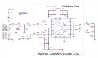
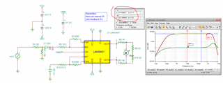
We are trying to design a single-ended to differential driver using the LMH5401. The final design needs to have a 10 V/V gain. We are currently testing on the eval board (LMH5401EVM). The user manual for this eval board states that "Inputs and outputs must be biased as in the LMH5401 datasheet (SBOS710) specifications for proper operation." (section 3.2). However we are having trouble identifying these biasing conditions in the datasheet. We are currently using AC coupled inputs and outputs, but are unsure if the default common mode voltage is the correct bias. Are we supposed to add some extra biasing circuit to the inputs? Our initial circuit is attached for reference. 

  • Since you are AC-coupled at both, input and output, the common-mode (CM) biasing should be an easier task than if things were DC-coupled. The key issue I see is the Vocm is set to 1.25V (2.5VB and R97/98 dividers) so without any input signal, each output will be sitting at 1.25V and close to the VOCRL condition.

    Considering input and output are AC coupled, to maximize signal swing, I'd suggest changing the VB voltage to VCC (5V) voltage so Vocm is sitting at 2.5V (midsupply).

    I have highlighted the key conditions from the LMH5401-SP datasheet/spec table to watch out for when biasing.

    Input CM voltage, which should be within the input CM low/high range, will be output CM voltage that is a scaled factor of Rf and Rg resistor network.

    Datasheet section 9.3.2.1 gives good insights into CM and input/output considerations.

    Thanks,

    Keyur

  • Also, if I set up for a gain of 10V/V,  50ohm matched with 305 ohm Rf values, these changes will hit that closer, 

    Rg3=Rg4 = 10.5ohm

    Rt1 = 1.02kohm

    Rm1 = 47.5ohm

  • And, I already had this file from early work, the VF1 is the input signal after the matching loss, yes, very close to -6dB. The Vm1 is the response to the load after 2X6dB losses, or 20dB-12dB = 8dB again, very close. The input signal rises above 1GHz as the internal CM loop rolls off, losing match. The main signal BW simulates to about 3.5GHz F-3dB

    And this file as TINA V9

    Gain of 10 LMH5401-SP test setup.TSC