This thread has been locked.

If you have a related question, please click the "Ask a related question" button in the top right corner. The newly created question will be automatically linked to this question.

INA186-Q1: INA186A1QDCKRQ1 Common-mode voltage

Part Number: INA186-Q1
Other Parts Discussed in Thread: INA186

hello,

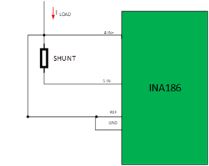
I have one question regarding the INA186A1QDCKRQ1 usage like the picture. We set the GND at the positive of shunt. That means that the potential of the shunt negative will be lower than GND. And the Common-mode voltage will also become negative. Is there any risk?

(P.S. the load current is 20A max and shunt resistance is 0.002ohm).

Thanks for your support!

  • Hey Karl,

    So is this a low-side application? Is the IN- side of the shunt actually connected to system ground.

    I am not sure this is a robust circuit you have currently. It seems like the INA186 GND pin voltage will change with Vshunt. I assume there is an MCU measuring Vout and that this MCU has its ground connected to system ground. So it seems like the ground of the INA186 and MCU will change according to Vshunt thus creating a variable offset in the measurement. The only way around this is to use a differential ADC that will measure the differential voltage between OUT pin and INA186 GND pin, as opposed to a single ended ADC

    The next issue is that the INa186 is set up to measure a negative shunt voltage, thus Vout will decrease as load increases. This means you cannot set REF pin to GND, or else OUT will just be saturating into the GND rail. In order to measure a Vshunt <0, REF must be >0, at least to REF = 40mV*20 + 0.1V = 0.9V. So at load = 0, Vout = 0.9. At load= 20A, Vout = -40mV*20 + 0.9V = 0.1V. Keeping V_REF >0.9V will ensure that Vout is always in its optimal linear region (see the gain error specification where testing conditions go from GND+0.1V < Vout < Vs-0.1V.

    Another option is to just set REF to Vs. This is same thing as setting REF to GND. The only difference is that you will have more variability in the Zero-current current output voltage (VZL, see datasheet specification table). When REF=GND and load =0A, Vout max = 10mV, but when REF=Vs, Vout min = Vs-40mV. It might actually be a little worse, because the swing-to-rail specification is tested where Vin exceed the max full scale range, so Vout is saturating/slamming into its Vs rail.

    Hope this all helps.

    Best,

    Peter

  • Hello Peter,

    Thanks for your support very much!

    Yes, it is a low-side application and the system GND is connecting IN+ of the INA186 like the picture show below.

    In this case, the INA186 is not set up to measure a negative shunt voltage. And there is no negative current at now use. This circuit achieves the desired effect and has normal function after testing. Only the common-mode voltage is below GND but not exceed the range of GND-0.2V.  So is that have any risk on this usage?

    The next issue is that the INa186 is set up to measure a negative shunt voltage, thus Vout will decrease as load increases. This means you cannot set REF pin to GND, or else OUT will just be saturating into the GND rail. In order to measure a Vshunt <0, REF must be >0, at least to REF = 40mV*20 + 0.1V = 0.9V. So at load = 0, Vout = 0.9. At load= 20A, Vout = -40mV*20 + 0.9V = 0.1V. Keeping V_REF >0.9V will ensure that Vout is always in its optimal linear region (see the gain error specification where testing conditions go from GND+0.1V < Vout < Vs-0.1V.

  • Hey Karl,

    So if the load current is flowing across shunt (from INP side to INN side, thus a positive shunt voltage) and there is a separate ground/return path for load current, then this circuit should be fine.

    I would ensure that the INA186 and MCU ground net is completely isolated from the load’s ground path because there will be voltage difference between them, specifically the Vshunt. I recommend this so there is no chance of a ground loop.

    Sincerely,

    Peter