A related question is a question created from another question. When the related question is created, it will be automatically linked to the original question.
If you have a related question, please click the "Ask a related question" button in the top right corner. The newly created question will be automatically linked to this question.
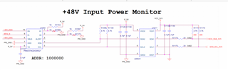
INA237-Q1: Help review the schematic design and give some suggestions
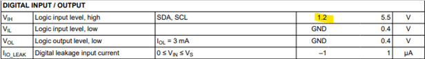
As Kai said, the INA237 can be powered by as low as 2.7V, so you could connect the INA237 directly to the 3.3V source. Additionally, the digital input levels are specified independently from Vs, and can go as low as 1.2V (see datasheet excerpt below) so the I2C isolator may be unnecessary in your case if you are only using it to interface between the high voltage levels.
The I2C address pins appear to be both pulled high in the schematic as R1080 and R1173 are DNI, please be aware that this will result in an I2C address of 1000101, not 1000000 as printed on the schematic. 1104 and 1097 must be set to DNI to drive A0 and A1 to ground level in order to set the address as 1000000.