This thread has been locked.

If you have a related question, please click the "Ask a related question" button in the top right corner. The newly created question will be automatically linked to this question.

THP210: Large value feedback resistors

Part Number: THP210
Other Parts Discussed in Thread: THS4561, TINA-TI, THS4551

Hello,

I plan to use THP210 for a energy power metering application. Sensor connected to THP210 present a very high output impedance (sensor are capacitors divider for kV voltage application).

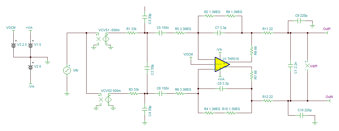
Then I should use very large value resistor for input and feedback. In the range of mega ohm.

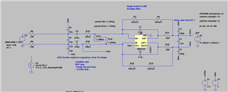
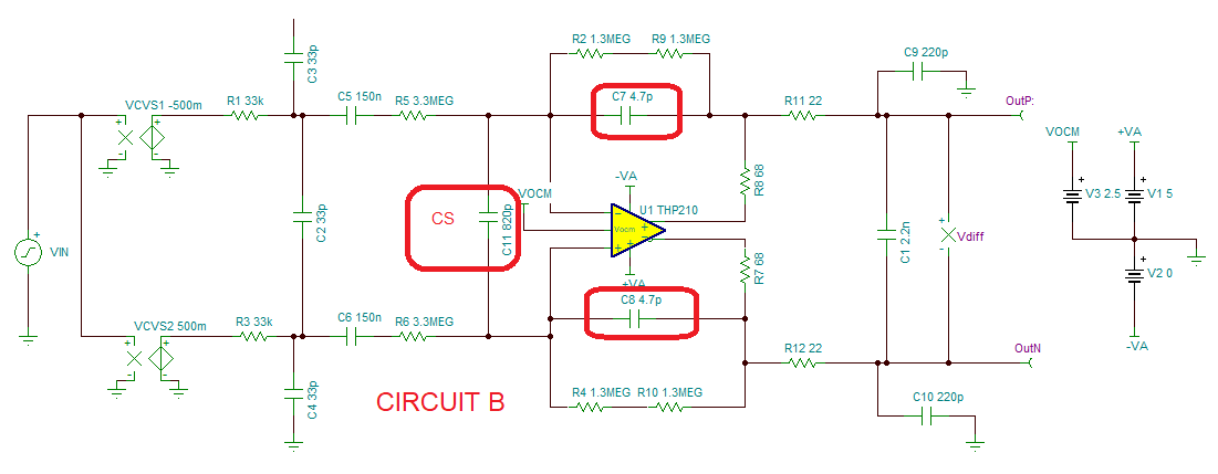
The THP210 will be used to made a single ended to differential conversion with a negative gain of approx -8dB.

Rin resistors about 3.3mega ohm, Rfb about 2.6 mega ohm and a small capacitor of 10pF in // with Rfb.

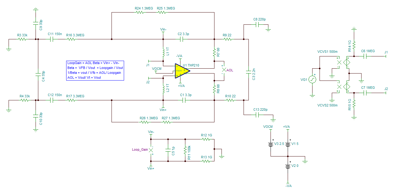
I will use a specific layout to avoid parasitic stray capacitance, especially in the area of inputs of THP210, I don't know if I should take another consideration to achieve a such design, but when I read following statement on datasheet I try to get the TI training but can't find it:

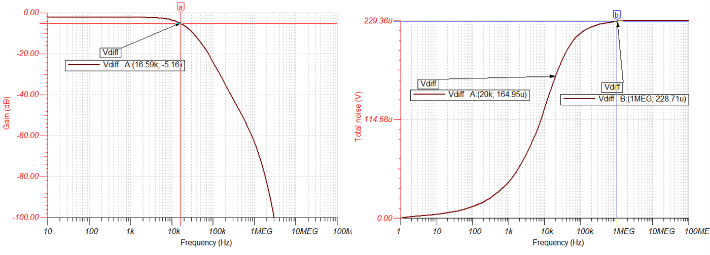
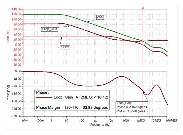
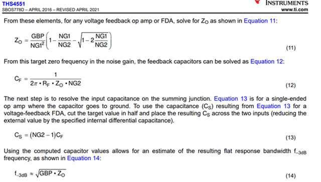
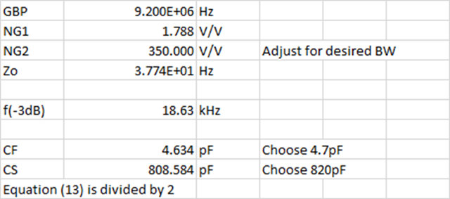
High feedback resistor values (RF > 100 kΩ) interact with the amplifier input capacitance to create a zero in
the feedback network. Compensation must be added to account for potential source of instability; see the TI
Precision Labs FDA Stability Training for guidance on designing an appropriate compensation network.

I can't find FDA stability training on TI website, the only video I found is relative to gain and phase margin, no mention of large value feedback resistor and stability.

If somebody can help me finding what kind of precaution I should take to get stability with large value of resistors using THP 210 ?

  • here is the schematic I plan to use

  • probably more than you want, but here is the original article on inverting compensation that applies here. Essentially your feedback cap and a diff C across the inputs of the FDA form the higher frequency noise gain where you want that to be 2 or greater usually. Also, not sure why you put the 100ohm inside the loop, I do that sometimes on a part like the THS4561 which is not super stable at unity gain, then I also tap the feedback C on the output side of the inside the loop R's. Also, those direct Cloads on the output might be a problem, may need some small R there to help phase margin. 

    https://www.edn.com/unique-compensation-technique-tames-high-bandwidth-voltage-feedback-op-amps-2/

  • Hi Briquel,

    I have performed the analysis of the original Circuit (A), and Circuit (B) with the compensation method adding the differential capacitor across the FDA inputs, as suggested by Michael.  Circuit (B) provides the best high-frequency attenuation for antialiasing purposes.

    Circuit A: Original Circuit (slightly modified)

    Using the circuit shown above with RFB=2.6MΩ and RIN=3.3MΩ, and the CFB at 3pF as shown on the schematic above. (I was not sure if you intended a 10pF or 3.3pf feedback, I performed the analysis using the 3.3pF feedback shown on the schematic)

    The circuit has an attenuation of -2.16-dB. The corner frequency of the complete circuit is about f(-3dB) = 16.6kHz.  I added 22Ω resistors at the output of the FDA, outside the feedback loop, to improve stability while driving the output 2.2nF kickback filter capacitor; and slightly reduced the resistors inside the loop from 100-Ω to 68Ω while verifying phase margin.

    Below is the slightly modified circuit, showing the AC small-signal frequency response, and the simulated total output noise in μVRMS:

    TINA-TI Circuit (A) frequency response and total output noise simulation file:

    THP210_CircuitA_closedloop_forum.TSC

    Stability analysis for Circuit (A):  The THP210 is stable with the 2.6MΩ feedback resistors, in this case, added the 22-ohm resistors at the output to ensure the FDA is stable driving the 22nF capacitive load at the output. I used the same method for open-loop stability analysis shown on TI precision labs. The simulation shows 63.9-degrees of phase margin.

    TINA-TI file for Open-Loop Stability Analysis for Circuit (A):

    THP210_CircuitA_stability_Forum.TSC

    Circuit B: Using Cs capacitor across the FDA inputs 

    Using the method that Michael S. has developed/suggested above. The method is also explained on the THS4551 datasheet.  Please refer to equations 11, 12, 13 and 14 and explanation on pages 45-48 on the THS4551 datasheet:


    Solving for the low frequency noise gain, NG1 = 1 + RF/RG = 1.788V/V, and gain bandwidth product GBP =9.2MHz for the THP210.

    Using excel, I modified NG2 as needed, to obtain a corner frequency f(-3dB) around ~18.6kHz (similar to the original circuit). 

    This yields the following results for CF and CS in excel: (using equations 11, 12, 13 and 14).

    Note:  CS equation (13) is divided by two in this calculation:

    Below is the circuit / simulation results for the AC frequency response, and total output noise in µVRMS.  

    The plots below show Circuit A and Circuit B frequency response and noise performance.

    Circuit B offers the -60dB/decade slope offering much improved attenuation for antialiasing purposes, with a trade-off in the total output noise:

    TINA-TI Circuit (B) frequency response and total output noise simulation File:

    THP210_CircuitB_closedloop_forum.TSC

    Also, I verified stability in circuit (B) providing 64.91-degrees of phase margin (stable).


    TINA-TI file for Open-Loop Stability Analysis for Circuit (B):

    6215.THP210_CircuitB_stability_Forum.TSC

    Thank you and Best Regards,

    Luis

  • Hi Luis, Michael,

    Wow, thanks for such fast answer ! it looks you missed the 1.6 mega ohm resistors providing a 3.3+3.3+1.6+1.6=9.8mega ohm total input impedance for sensors.

    Also the single ended to diff feature is not present on the tina simulations (one of the input pin connected to vgnd - 2.5VDC).

    Anyway if I add a capacitor on opa input this capacitor will be in // with the two 1.6mega ohm resistors.

    Will add resistors footprint between outputs of opa and fb path.

  • Hey Briquel and Luis, 

    I see also that Luis has tapped the feedback C off the output side, which is better and added an iso R in the output to the cap loads. Those are also good ideas, 

    There is also a section I put into the THS4551 datasheet that is pertinent, "Designing attenuators" section 10.1.6. 

    I was wrestling with stability issues in even the simple MFB filter designs. I had done the front page THS4561 circuit before I really appreciated how the resonant open loop Zo was getting into the loop phase margin via the feedback C required in the MFB, here I re-worked that design, 

    7450.THS4561 front page MFB updated ckt Aug2018.docx

  • Thank you Briquel and Michael,

    Kind Regards,

    Luis

  • Many thanks sir, especially for the shared Tina files, which saves me lots of time!

  • Hi Briquel,

    Thank you, Happy to help,

    Kind Regards,

    Luis