This thread has been locked.

If you have a related question, please click the "Ask a related question" button in the top right corner. The newly created question will be automatically linked to this question.

TL331: TL331KDBVR TIKG vs T1K8

Part Number: TL331
Other Parts Discussed in Thread: , LM2903-N

hi teams:

1.For TI part with MPN TL331KDBVR, we encountered 100% ICT test failure,  all failed material Device Marking is TIKG, after performed the material swap validation, the failure symptom follows TI device. We swapped the old Device Marking T1K8  and retested, the failure symptom has been solved, we want to know any difference between TIKG and T1K8  ? any  PCN? 

2.TIKG(Device Marking )

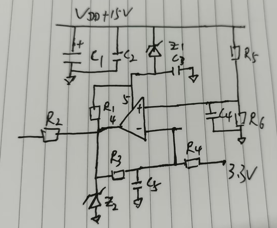
As shown in the following figure, the customer can also solve the problem by replacing R1 from 10K to 47K,

I want to know which parameter of TL331KDBVR will be affected by changing R1.

参数如下:

C1:100uF    C2:100nF C3:100nF C4:  10nF C5:10nF

 R1: 10K   R2: 10R  R3:1M  R4:   10K  R5:100K R6:31K

Z1 and Z2 are 3.3V voltage regulators

 The difference in output capacitance, output impedance, and driving current between T1KG and T1K8 chips (measured value)

  • Hi Kevin,

    Thanks for your post. Yes, TL331 family is undergoing PCN so it is you may be receiving a mix of the old and new die when ordering the TL331. This new die is the same die as the "TL331B" device. See the document here: Product Change Notification (PDF) . To tell which is the old die and which is the new die, you can look at the assembly site code "CCO" field on the box label. If it says "USA", it is the old die. If it says "CHN", then it is the new "B" die. The main differences between TL331 and TL331B can be found on the front page of the datasheet. The new die has much lower bias current which would affect the resistor network. It looks like the input common mode range is being violated. Can you show waveforms of the inputs and outputs and the supplies of each pass and fail case? 


  • hi :

    1. Confirmed :die is  "TL331B" device

     2.  It looks like the input common mode range is being violated

      reply:According to the schematic diagram, the maximum voltage between V - and V+ is 3.6V, the power supply voltage is 15-3.3=11.7V, and the maximum input common mode voltage is 11.7-1.5=10.2V. It should not exceed the maximum allowable common mode voltage

     Is this how to explain the common mode voltage range?

  • Hi Kevin,

    shall this be an oscillator? Are you sure that the schematic is drawn correctly and that the given component values are correct?

    R6 and R6 produce a voltage of 3.55V at the +input. To allow the output of TL331 to toggle, the output voltage must be able to exceed 3.55V. So, "Z2" must not be a 3.3V zener diode. If the circuit still works, then only because "Z2" shows manufacturing tolerances.

    Keep in mind, that 3.3V zener diodes are highly non-ideal (compared to 6.8V zener diodes, e.g.) and show only a very soft knee in the current versus voltage curve. There's no abrupt change at all and the voltge drop caused by a certain flow current can drastically vary from diode to diode and with temperature.

    To make the voltage drop across "Z1" more immune against supply current changes of TL331 and of the circuit (R1 !), you could think about adding a dummy load from the anode of "Z1" to signal ground and by this to force a more constant current to flow through "Z1". Another improvement could be achieved by uncoupling "Z1" and "Z2" from each other. Right now they are coupled via R1. And you should think about zener voltage of "Z2" and/or the set threshold voltages of TL331.

    If this really is an oscillator, then you should also provide hysteresis as shown in figure 17 of datasheet of LM2903-N, e.g..

    So, beccause your circuit is non-ideal, even the least and subtly change will make the circuit stop working properly. This is not the fault of TL331.

    Kai

  • Hi Kevin,

    What is the actual function of the circuit? What are you trying to achieve?

    Also as Kai remarked, Zeners should have a minimum amount of current to maintain regulation. Here every time the output goes low, the load on the Zener changes. This will cause the supply votlage to fluctuate. The 100nF cap may not be big enough to hold the supply stable enough for proper operation.

    Also, the new "B" die does have about 200uA less supply current, so there is less pre-loading of the Zener.

    Just power the comparator directly off the 15V supply...that give you even more input range.

    Are you trying to limit the output swing with the Zeners?