Other Parts Discussed in Thread: ALM2402F-Q1, , OPA564-Q1
Hello all,
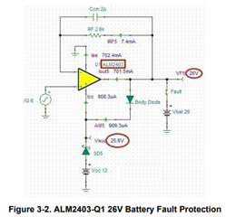
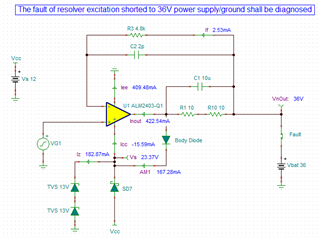
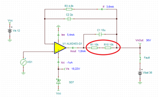
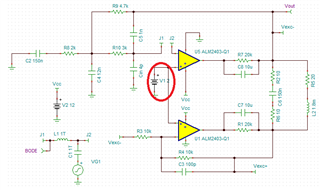
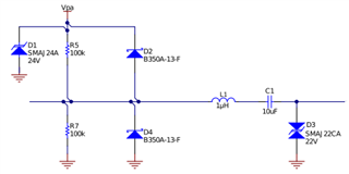
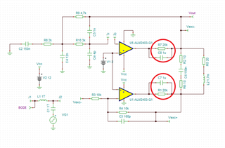
in my resolver application I need a shortcut protection to 36V for at least 60s, in the application note (SBOA447) following design is suggested:
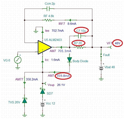
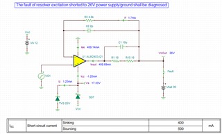
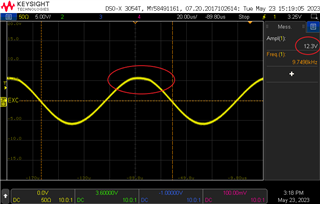
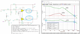
a 20Ohm R7 Resistor in placed inside the feedback loop and bypassed with a 10u capacitor, C7. At the typical frequency of 10kHz used in most automotive resolver excitation applications, the impedance of
10uF bypass capacitor is around 1.6Ω
It's a genius idea, but I still have 2 problems:
1. the TVS 26V can't hold for 60 seconds,
2. and the power dissipation at the R7 would be very high --> 5W~7W
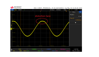
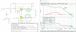
so what if I just increase the R7 to 20kohm? Or even delete the R7, just left the C7?
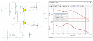
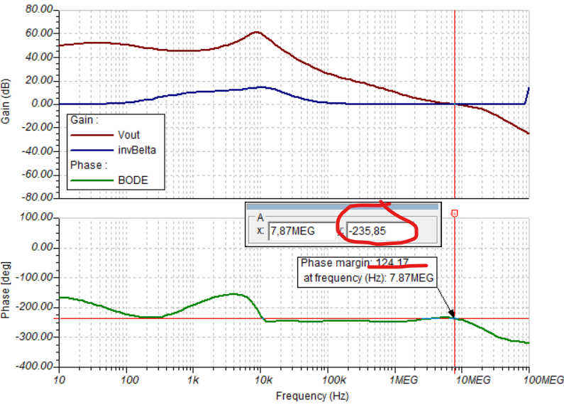
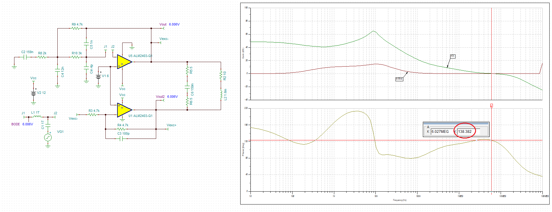
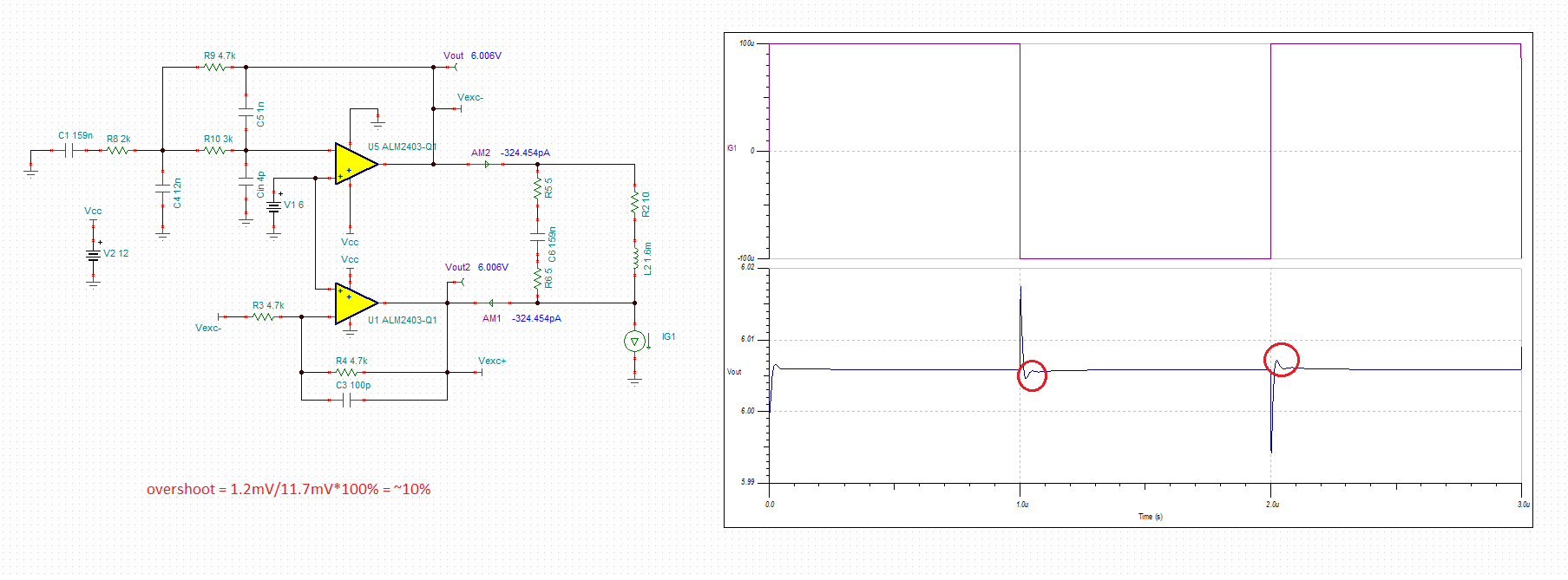
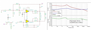
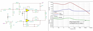
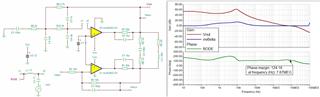
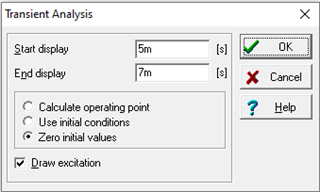
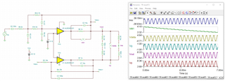
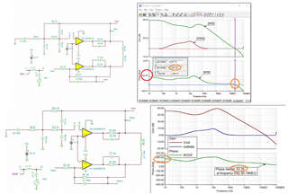
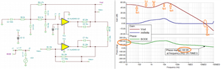
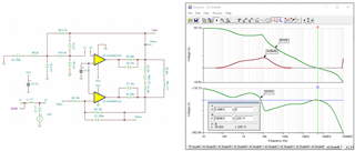
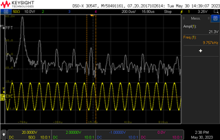
According my simulation,
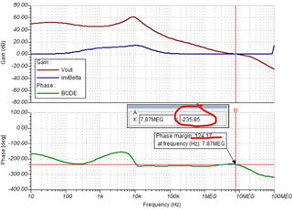
The Phase margin is 124.17 (or -235,85??), so I believe with 20k R7 is no problem, is there anything error in my design??
BR
Jin