This thread has been locked.

If you have a related question, please click the "Ask a related question" button in the top right corner. The newly created question will be automatically linked to this question.

THS4551: ground plane guide

Part Number: THS4551
Other Parts Discussed in Thread: OPA810, ADS127L11

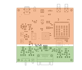
Top area is digital circuit, FPGA, DDR ram, 4G module, eMMC and so on.

bottom area is analog circuit, amplifer opa810 + ths4551 + ads127L11

question: how to handle the gnd? should I two separate gnd: digit/analog , and then connected to one point? or just common gound for digital and analog?

  • Hi Liping,

    Although there is not a definitive way to design a PCB board, we recommend using one common ground plane for the layout and taking extra precautions in separating your digital and analog components to minimize noise caused by digital signals. Having a split layout is possible, however it is much harder to implement correctly. Numerous issues arise when signal traces pass over plane gaps causing EMI and crosstalk, making the layout of the board more difficult. Voltage differences between the AGND and DGND can also cause problems to certain IC components. For this reason, we recommend a solid ground plane with short return paths to ground as well as separating the digital and analog components to different sections on the PCB.

    I will also add a link to a great E2E article discussing these ideas. I highly recommend looking over the information provided in the discussion as it also highlights very good references to this question. The E2E thread can be found here.

    Best Regards,

    Ignacio