Other Parts Discussed in Thread: TINA-TI
Apologies in advance if these are mundane specs or queries… I have only briefly worked with ideal op-amp theory in the past (roughly 4+ years ago). If my following queries should be on a separate forum post(s), please let me know and I will break up these queries.
I have been configuring a photodiode amplifier that uses the LMP7721 op-amp (for now). It is my first time designing/simulating a transimpedance amplifier circuit and so I have been trying to read-up the following forum/documentation to understand the significance/importance of op-amp parameters listed in the typical datasheets:
- https://electronics.stackexchange.com/questions/684615/how-to-determine-whats-a-suitable-opamp/684622#684622
- LMP7721 datasheet
- TI’s “Understanding Op-Amp Specifications” document (www.ti.com/.../sloa011b.pdf
- e2e.ti.com/.../5019621
TLDR: I am having trouble interpreting the relation/significance of the input common-mode voltage range (CMVR), common-mode rejection ratio (CMRR), and power supply rejection ratio (PSRR). How do these values help with selecting the appropriate supply voltage values/range to power an op-amp (such as the LMP7721)?
Detailed comments/questions:
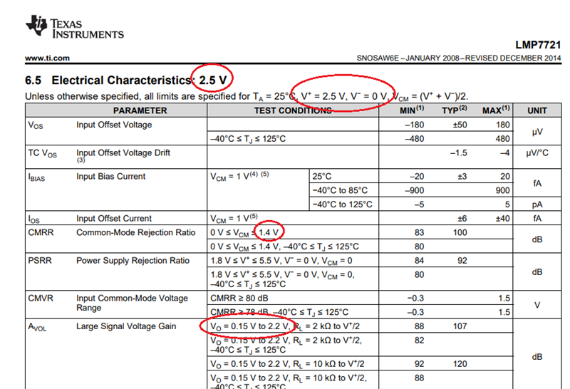
For CMVR, my interpretation of this parameter from pp. 11-13 of document 3., leads me to believe that it is a limitation to the voltage applied to the supply pins (V+ or V- ) based on the voltage applied to VIN- and/or VIN+ where (for example) if V+ >> VIN+ then the op-amp won’t amplify the signal or operate at all… however, the LMP7721 datasheet (p. 5) simply quotes the CMVR as a max (1.5 V) and min (-0.3 V) values. Are these max and min CMVR values what V+ must be less than for the op-amp to operate/amplify a signal?
For PSRR from document 3 mentions it is a ratio between the output voltage and supply voltage “Vcc”. Is this just another way of saying what the supply voltage needs to be for proper operation of the op-amp? The datasheet of the LMP7721 (p. 5) mentions that it is tested for 1.8 V ≤ V+ ≤ 5.5 V, V- = 0 V, VCM = 0, which is the supply voltage range (Vs) quoted for the LMP7721. (Also, how is VCM = 0 when V- ≠ V+ ?)
For CMRR, the best I can gather from document 3., is that the offset voltage of the input pins (VIN- and VIN+) changes due to the amount of gain that is occurring. However from p.5 of the LMP7721 datasheet (and from 4.) I interpret this parameter as the range of voltages applied to the supply must obey (V-) < Vcm <(V+)-1.1V (for +/- 2.5V supply) for the op-amp to operate appropriately. Does this parameter imply that for combinations of (V+ or V- ) that do not adhere to the inequalities obey (V-) < Vcm <(V+)-1.1V the op-amp simply does not operate?
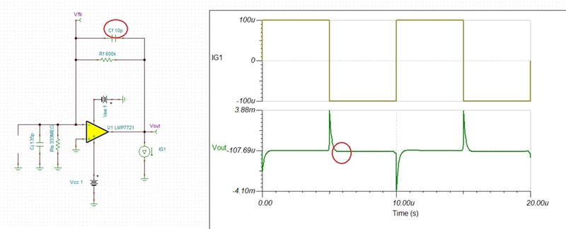
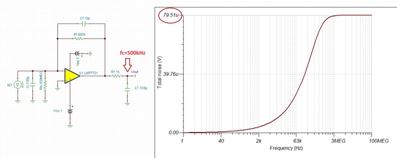
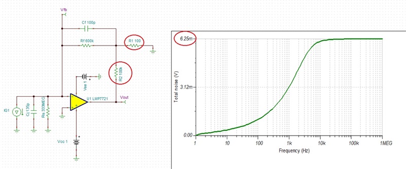
I tried using TINA-TI simulations along with information on a past TI forum post (e2e.ti.com/.../5019621 to learn/experiment with various supply voltage configurations that work for my TIA. I attached the same TINA-TI file to this post. Below are snippets of my TIA design and oscilloscope reading of Vout for an inputted 15 pA square wave (IG1). From this experiments/simulation I concluded/ came to the question of:
Why do I need to apply a negative voltage to the negative supply rail (V-) to get a valid input from the LMP7721? And how does this relate to CMRR, and CMVR?

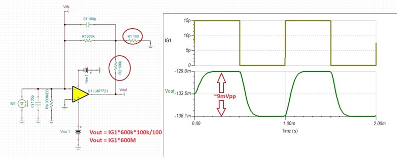
Supplied +/- 1.5 V to the supply rails (Vcm = 0). It obeys my interpretation of CMRR as -1.5 V < 0 < 0.4 V. as such the oscilloscope reads and actual square wave signal.
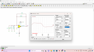
Supplied +/- 1.0 V to the supply rails (Vcm = 0). It does not obey my my interpretation of CMRR as -1.0 V < 0 < -0.1 V. the oscilloscope still reads and actual square wave signal.
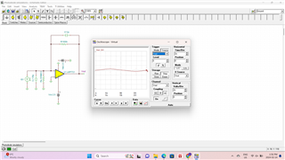
Supplied + 2.5 V & 0.0 V to the supply rails (Vcm = 1.25). It does not obey my interpretation of CMRR as 0 V < 1.25 V < 1.4 V is valid yet the oscilloscope does not read a square wave signal with ~ 9uV amplitude.

Supplied + 3.0 V & - 0.5 V to the supply rails (Vcm = 1.25). It does obey my interpretation of CMRR as -0.5 V < 1.25 V < 1.9 V is valid and the oscilloscope does read a square wave signal.
Acknowledgment: the TINA-TI file used here is an edited version of a file found on the following forum: e2e.ti.com/.../lmp7721-clarifications-on-input-protection