Other Parts Discussed in Thread: TINA-TI
Hi
I am using TLV9056 as a differential amplifier to amplify the output from the current transformer (1:1000) the noninverting pin is biased with 3.3V and the Gain is ~50.
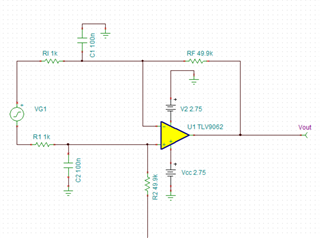
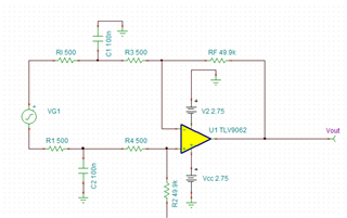
Refer to the schematic below :
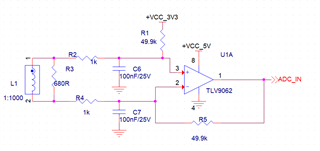
While testing, we observed that when OP-AMP is not powered ON there are no 3.3v and 5v on the circuit, the out of the CT measured across the R3 is as per design cals, but when the circuit is powered on the input differential voltage dips and with increasing in input voltage signal, the dip also increases.
Refer to the following waveforms :
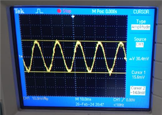
Test 1.
a. Waveform when the board is powered off.
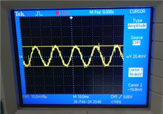
b.Waveform when the board is powered on.
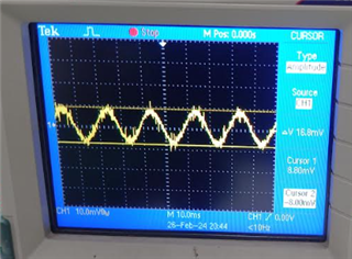
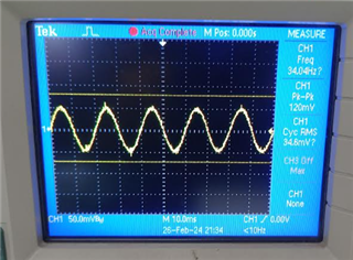
Test 2.
a. Waveform when the board is powered off.
b.Waveform when the board is powered on.
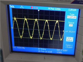
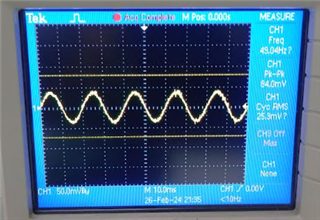
Test 3.
a. Waveform when the board is powered off.
b.Waveform when the board is powered on.
Please let me know the reason for this behavior and what is the workaround for the same.
BR
Chaitanya