The TI E2E™ design support forums will undergo maintenance from July 11 to July 13. If you need design support during this time, open a new support request with our customer support center.

This thread has been locked.

If you have a related question, please click the "Ask a related question" button in the top right corner. The newly created question will be automatically linked to this question.

TLV9002: TLV9002IDR application issue

Part Number: TLV9002

Hi Team,

I have encountered some problems when using TLV9002IDR and would like your help to confirm:

Please refer to the application circuit in the figure below, where U2-A and U2-B are TLV9002IDR, used for output load adjustment.

U2-A serves as the voltage follower of the MCU command signal.
U2-B compares the MCU command signal with the load current and outputs an adjustment MOSFET Vgs to control the load current.

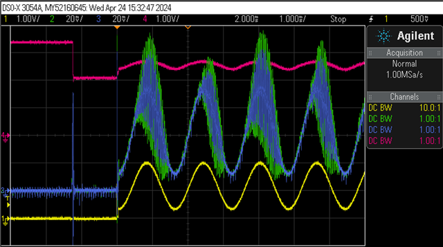
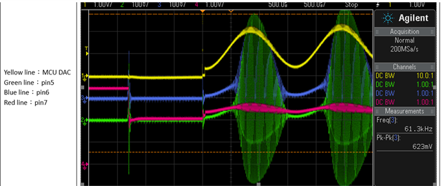
However, it was found that when TLV9002 Pin.1, Pin.2, Pin.3, Pin.5, and Pin.6 were all 0V, Pin.7 output a voltage of 3.3V, causing the MOSFET to malfunction.

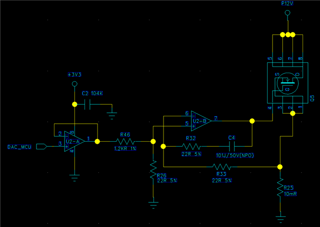
Please help confirm that TLV9002IDR is in the application circuit:

1. Are there inappropriate matching parameters that need to be adjusted?
2. Or is it due to the inherent characteristics of TLV9002IDR that it is not suitable for this application and the materials need to be replaced?

Regards, thank a lot.

  • Hi Rock,

    Does the current drive circuit work as expected for voltages other than 0V from MCU DAC? If so, can you provide voltages at pin 7, pin 6 and pin 5 during normal operation?

    What is the part number for Q5, and what is the component value for C4? 

    This additional information will help me simulate the circuit operation.

    Thanks,

    Jacob

  • Hi Jacob,

    Please refer to the reply. Thanks.

    Q5 Part number: Lead Power- LM1A039NAK8A

    C4: 100pF

    When the MCU DAC outputs signals other than 0V, the circuit cannot operate as expected, and the MOSFET Ids will oscillate. Please refer to the waveform during operation in the figure below:

    Yellow line: MCU DAC, Green line: pin5, Blue line: pin6, Red line: pin7

    LM1A039NAK8A_datasheet.pdf

  • The red line does not show oscillations.

    The voltage at pin 5 should not be oscillating. I wonder if the noise is coupled in from the power supply (VCC or GND). Try adding a small capacitor in parallel with R26. (R46 and that C form a low-pass filter.)

  • Hi Rock,

    Thanks for all the details here, it is helpful to see the waveforms at the terminals of the amplifier. 

    Pin 7 looks to be relatively stable, maybe slightly noisy in part due to the IN+ voltage also having noise coupling into the amp. I agree with Clemens, a LPF may help with this a bit. 

    It looks like the FET is able to provide a feedback signal to the amplifier via R25 and R33. What does the Ids look like? It looks to me like the amplifier is operating as it should be.  

    Thanks,

    Jacob

  • Hi Jacob,

    Try adding a 470pF capacitor to R26, and the waveforms become more divergent as shown below.

    Does the added capacitance become a path for noise transmission? Or is the capacitor causing TLV9002 instability?

  • Hi Rock,

    Did you pull R26 and put the 470pF cap, or put the 470pF cap in parallel with the existing R26?

    Yes, it is possible that the capacitor is acting as a low impedance path for high frequency noise to couple into pin 5. Alternatively, maybe this is acting as a path for the noise to couple into the ground plane, and then disturb the output of the amplifier through the power supply pins. 

    This relatively small capacitor will not destabilize the amplifier when we have the 1.2kOhm resistor isolating the output from the cap load. 

    Important to note, I see the same frequency signals on the MCU DAC signal. I would not expect the MCU_DAC signal to be this noisy. It is possible that all of our problems are coming from this trace? In an ideal world, this ADC has a charge bucket filter on the output. Is this pin directly connected to pin 3 of the op amp?

    Thanks,

    Jacob