This thread has been locked.

If you have a related question, please click the "Ask a related question" button in the top right corner. The newly created question will be automatically linked to this question.

INA296B: About Accuracy

Part Number: INA296B
Other Parts Discussed in Thread: INA296A

Tool/software:

Hello,
Thank you for your help.
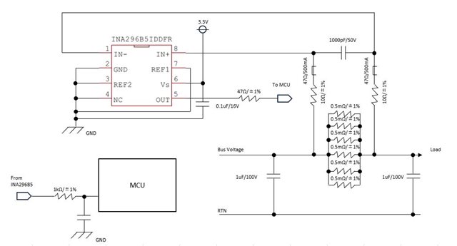
We are designing the attached current sense circuit using INA296B5.
The accuracy of low currents of 1A to 20A may exceed ±2%.
Is there any suggestions to reduce the accuracy to less than ±2%?

  • For 1 A, the voltage drop over the shunt resistor is 83 µV.
    For 20 A, the voltage drop over the shunt resistor is 1.67 mV.

    The INA296B5's input offset error can be up to 150 µV. This is more than the 1 A signal, and 9 % of the 20 A signal. And it does not yet include the resistor tolerances or the gain error.

    The INA296A‍5 would have a much smaller offset voltage (max 8 µV).

    You could also use a larger shunt resistor value, but I guess the voltage drop or power dissipation would be too large.

  • Hi Clemens,

    Thank you for your support.
    There are 10Ω/±1% resistors and 47Ω/500mA beads as filters between the shunt resistor and IN+, IN-.
    Will the accuracy improve by removing the filters?

    Regards,

  • The input bias current is about 35 µA. This results in a voltage drop of about 2 mV over these resistances. You get errors only if the bias currents of the two inputs do not match. It might be worthwhile trying to remove them.

  • Hello Tamaki,

    Layout of the resistors also matters as you would want the average of the current on all those resistors.  The layout could make it so that more current is on one resistor more than others.  The solder could include more resistance and variation on each resistor could vary, and where you sense the voltage will impact this.

    Your series resistance will impact as you can see the INA296 does change IB vs Vsense voltage.

    Regards,

    Javier

  • Thank you for your support.
    We will also try changing the layout to take into account the effect of the connection from the shunt resistor.


    Regards,

  • Hello Javier,

    Thank you for your support.


    When changing the layout,
    ・if the sensing lines are routed through vias on multiple layers of the board, should they be routed on layers as close as possible?
    ・Or should they be routed so that they overlap when viewed from above, forming pairs between layers?
    ・When using 5-10 shunt resistors in parallel, is it better to place the sensing line closer to the center so that it can detect a current closer to the average?
    ・Would it be more effective to shorten the sensing line to the amplifier with compensation in mind?

    Regards,

  • Tamaki,

    Thank you for your patience. Javier is out of the office today but will reply when he returns on Monday.

    Louis

  • Hello Tamaki,

    Below are some notes with some images.

    ・if the sensing lines are routed through vias on multiple layers of the board, should they be routed on layers as close as possible?

    This is less important as to where you sense on the resistor pads.  See red circle in drawing.

    Or should they be routed so that they overlap when viewed from above, forming pairs between layers?

    You should have some resistance between the resistors and can be as simple as thin copper traces.

    ・When using 5-10 shunt resistors in parallel, is it better to place the sensing line closer to the center so that it can detect a current closer to the average?

    The image below shows the best way to get the average.  The series resistance helps get the average.

    ・Would it be more effective to shorten the sensing line to the amplifier with compensation in mind?

    Like my image below states you want to add some resistance to the sense lines to get an average voltage drop across all resistors.

  • Hello Javier,

    Thank you for your detailed explanation.
    We will take it into consideration.