


We an issue with our VCA820 circuit not matching the results we see in TINA
We implemented an AGC loop based on the circuit shown Fig 83 (page 22) of the VCA820 datasheet with some minor changes differences, we simulated the circuit in TINA, but we are not seeing what we expected on the board.
Included with this post are several captures showing the problem as well as the simulation model.
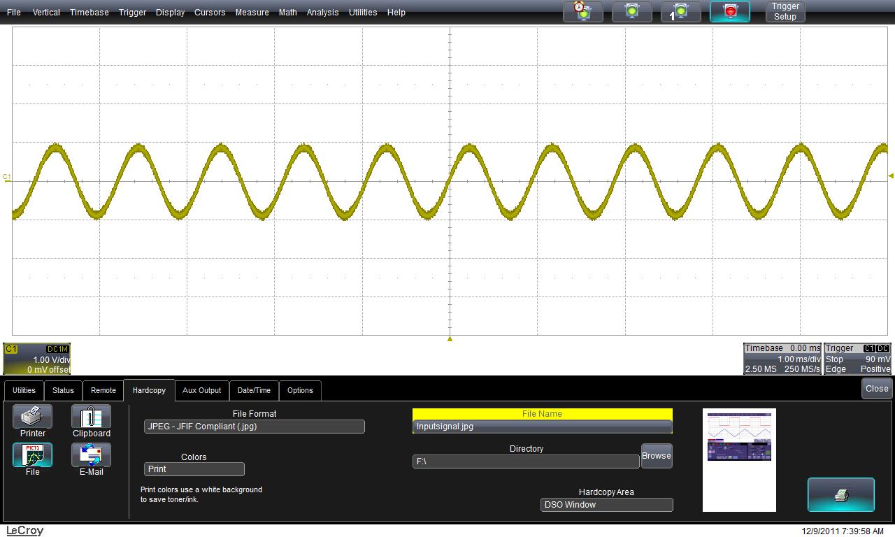
The input to the circuit is a 2V pk-pk signal, 0 offset (shown on inputsignal.jpg)
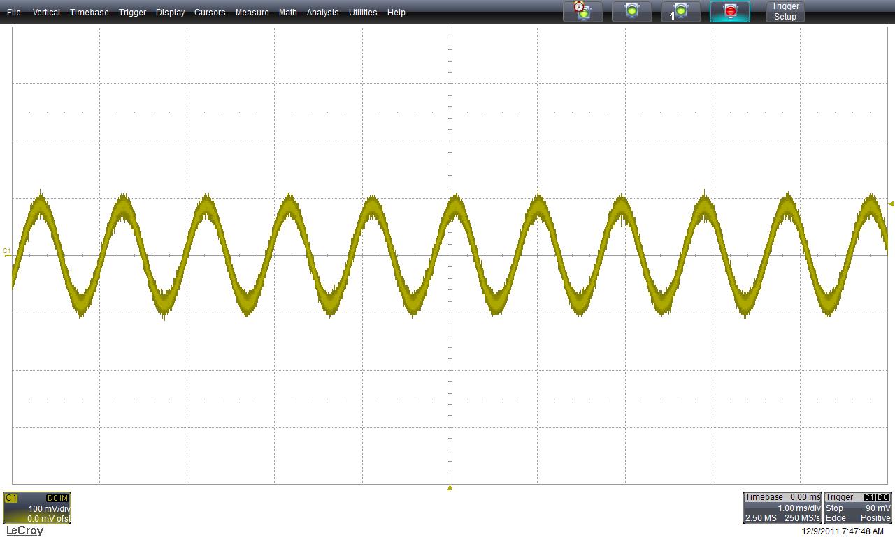
The input to the VCA820 is a 200mV pk-pk signal, o offset (shown on vca820pin.jpg)
Output of VCA820
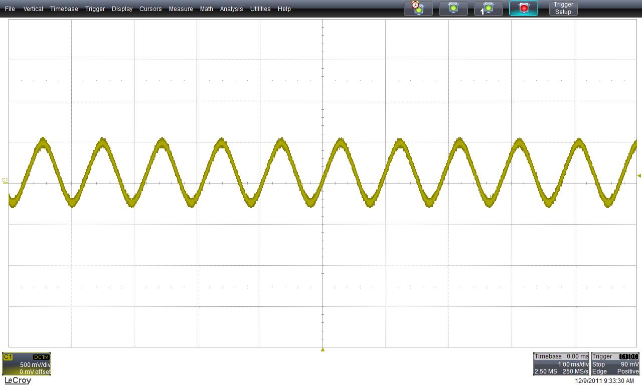
The output of the circuit is a 3V pk-pk signal with some offset (shown on opa695pin6.jpg)

The expected output was a 5V pk-pk signal with little to no offset.
Test have been run with multiple boards.
All component values have been verified.
Any input TI could provide would be greatly appreciated.


