This thread has been locked.

If you have a related question, please click the "Ask a related question" button in the top right corner. The newly created question will be automatically linked to this question.

THS4131 Single to Differential

Other Parts Discussed in Thread: THS4131, ADS8363, ADS8363EVM, THS4130

Hi,

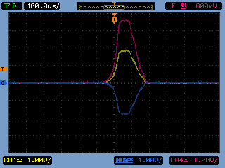
We are using THS4131 to convert single ended signal to differential signal to drive ADC ADS8363 (EVM). We have connected positive and negative supplies (+5v, -5v). The Vocm is not connected.

We see half the input signal on Vo+ and Vo- outputs.  

For the ADC we have Ao+ to Vo+ and Ao- to Vo-. Vref is connected to 2.5v. 

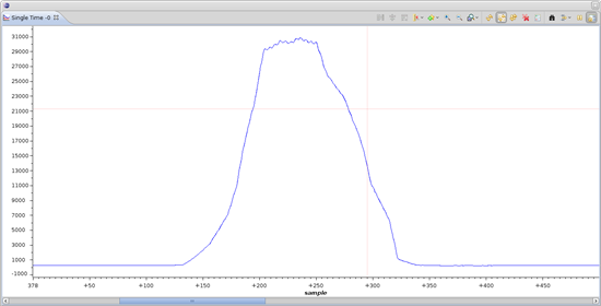
When we connect the input signal that varies from 0-5V, we see 2.5 to 5V after the ADC (samples are from 0 to 32767 instead of -32768 to 32767).

How can we get the full range?

Best Regards,

Basu 

  • Basu,

    Can you use one of the other inputs of the ADS8363? Based on the schematic on page 6 of the user's guide for the ADS8363EVM it looks as though the A0- jumper on the is not actually connected to ground. Try connecting to A1+ and A1- and see if this solves the problem.

    Another option would be to solder the other side of A0- (pin 15 on J1) to ground with a wire.

    Regards,
    Luke Lapointe
    High Speed Amplifiers

  • Hello Luke,

    We have the pin grounded. But we don't think thats a problem. It should be something else. 

    Best Regards,

    Basu 

  • Basu,

    If you are using +/-5V supplies with the Vocm pin floating, then the output common mode voltage will be set to 0V.  If the ADC is being powered on 0V to 5V, a signal swinging around 0V would be clipping on the negative side. Can you provide some scope shots of the input and output of the amplifier as well as what the ADC is seeing?

    Thank you,
    Luke Lapointe
    High Speed Amplifiers

  • Hello Luke,

    With +/- 5V, this is the output we see from the amplifier.

    Ch4: Input (Pink)

    Ch1: Vo+ (Yellow)

    Ch3: Vo- (Blue)

    ADC:

    Vo+ is connected to Ao+ and Vo- is connected to Ao-. 

    ADC ref: 2.5V

    Vocm is not connected. 

    The ADC values are shown in the plot below:

    Hope this helps.

    Basu 

  • Basu,

    Vo- is swinging below 0V. If the ADC is only powered on 0V to 5V, this signal will be clipped and you will only see half of the signal. Try applying 2.5V to the Vocm pin of the amplifier and see if that helps.

    Regards,
    Luke Lapointe
    High Speed Amplifiers

  • Hello Luke,

    Our signal is 0-5v single ended. 

    We need full range (0-5v) signal after ADC for processing.

    We are using ADS8363 to digitize it. It is powered with 5v supply.

    We are using THS4131 to convert the single ended input signal into differential signal so that we can use the ADS8363. The THS4131 can be powered with +/- 5V or only +5V. We are fine with either option.

    When we look at the signal after ADC, we only see half the range (0-2.5V). 

    What are we missing? Should we use any other amplifier? 

    Thank you

    Basu 

  • Basu,

    The data converter is not seeing the signal on the Vo- because it is swinging below 0V. You need to add an offset to the output of the amplifier to center your signal in the middle of the ADC's range. If you apply 2.5V to the Vocm pin of the THS4130, then the output will be centered at 2.5V. For a 0-5V single ended input signal and a gain of 1, this would translate to a 0-5V differential output signal, or 0-2.5V on Vo- and 2.5V-5V on Vo+.This way, the ADC will be able to see both the positive and negative inputs from the amplifier and be able to use the full scale range of the data converter.

    Another thing to note is the input common mode range of the THS4130 is Vs- + 1V to Vs+ - 0.5V. This means that if your signal is 0V to 5V, you could be clipping the upper end if you are using a gain configuration of 1. You might want to adjust your supplies to give yourself some margin. For example, you could use Vs+ = 7.5V, Vs- = -2.5V. Another option would be to attenuate the input signal and use a gain to avoid this limitation as well.

    Regards,
    Luke Lapointe
    High Speed Amplifiers

  • Hi Luke -

    I'm working with Basu on this little problem here.  I think we've come to an understanding of what is happening - I'd just like to try to explain it here to make sure I'm looking at it correctly!

    (We are using Vs+ = 5V, Vs- = 0V, Vocm = 2.5V).

    The trick is how you look at a differential signal, and what it means to have a positive and negative differential signal.  We have an input signal that is single ended, has a range of 0 - 5V, and is referenced to GND.  When we use the THS4131 to convert this to a differential signal, we see Vo+ showing half the signal above Vocm and Vo- showing the other half of the signal inverted below Vocm.

    This means that we only ever see a positive differential signal, which shows up as a (positive) half scale result on the ADC (from 0 to +32768).

    What we should be seeing is the differential outputs flipping between positive and negative around Vocm as the input signal passes Vocm.  This would give us a differential signal that has both positive and negative values, and would give us the full range on our ADC (from -32768 to +32768).

    I'm not sure why it is behaving that way.  What we might do to solve the problem is leave the input as single ended and connect the ADC V- pin to the 2.5V reference.  This will result in the ADC seeing a differential signal that swings between -Ref to +Ref, and gives us a full scale digital result (-32768 to +32768).

    I hope that makes sense.  Thanks for your help.

    Joe.

  • Hello Luke,

    Here is another attempt to explain what we are seeing. I have attached a pdf file showing our connections. 

    Please let me know if we missing anything or the diagram is not clear enough. 

    3644.SCAN0001.PDF

    Thank you.

    Basu 

  • Basu,

    After looking at your attachment I've noticed a couple things. First, the datasheet for the ADS8363 specifies a full scale input range of -Vref to +Vref. This means that the peak to peak differential voltage should be 5V centered at 0V to get the full scale range. In other words, differential voltage at the two converter inputs should never exceed 2.5V and should never be below -2.5V. In the diagram that you attached, the differential voltage seen at the input of the ADC ranges from 0V to 5V, which exceeds this range. Also, because the input common mode is 0V and you have a positive pulse, the output will only ever swing positive. To fix both of these problems, you can apply a bias voltage of 2.5V to the unused input. (see attached)

    1212.THS4131 + ADC.TSC

    Adding 2.5V to the negative input will bias the input common mode to 2.5V which will effectively shift the input common mode to the center of the pulse, allowing the amplifier to swing both positive and negative. Then when you apply 2.5V to the Vocm pin, each single ended output will be centered around 2.5V, swinging from 1.25V to 3.75V for Vo+ and 3.75V to 1.25V for Vo-. This will still result in a peak to peak differential voltage of 5V, but now the differential voltage will be swinging from -2.5V to 2.5V, which is consistent with the ADC's full scale input range.

    Please let me know if this fixes the issue.

    Regards,
    Luke Lapointe
    High Speed Amplifiers