This thread has been locked.

If you have a related question, please click the "Ask a related question" button in the top right corner. The newly created question will be automatically linked to this question.

Plz explain this buffer circuit ...

Other Parts Discussed in Thread: RC4558

 Hi

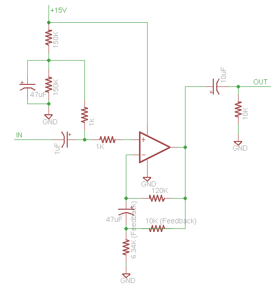
I'm stuck trying to understand a part of this and would appreciate any pointers from you. This is a working circuit and reproduced as it is. 

a) The input 1uF capacitor (connected in reverse) - this is a polar cap but am not sure how this configuration works.

b) The 120K resistor and 47uF capacitor in the feedback loop - is that for nulling the offset ?

Thank you and regards


  • Hi, Soumitra,

    I am going to move your post to our precision amplifier forum.

    In the meanwhile, I might suggest you throw this in TINA and run some sims. Do a frequency sweep of the input.

    I'd assume the polarity of the 1 uF cap just says the bias of the pre-stage is at a lower voltage than the bias of the input of the op amp.

    -d2

  •  Hi Don

    Thank you for the reply.

    Yes the polarity seems logical considering the bias potential but could it not have been better to have a non-polar capacitor there ? 

    Let me run a TINA sim and get back.

    Thank you and regards

    Soumitra


  •  Hi Don

    Im afraid im a newbie to TINA, though i did setup the scene and ran an AC and DC analysis to begin with.

    The voltage at points are probably not correct - the midpoint of the resistor divider shows 11.1V whereas it should be 7.5V. I have attached the file here in case it can be opened by others to verify. The opamp used in the original circuit is a JRC4558 ... and the equivalent available with TI is the RC4558 whose supply is lower than the NJR opamp.

    Any help is much appreciated.

    Regards

     Soumitra3264.Input Opamp Test.TSC