This thread has been locked.

If you have a related question, please click the "Ask a related question" button in the top right corner. The newly created question will be automatically linked to this question.

Building a simple circuit to detect electrical contact

Other Parts Discussed in Thread: TLV3401, TINA-TI

Hello,

I am trying to build a simple circuit that can detect whether a conductive nanoscale cantilever probe (basically, a sharp needle) is touching a bare Au substrate. Currently, I have used one of TI's op-amp evaluation boards (Area 100, page 2-3 here: http://www.ti.com/lit/ug/slou062a/slou062a.pdf), and built a non-inverting amplifier using a LF411CN.

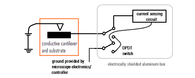
The circuit diagram is shown here:

Do you have any suggestions as to how I can improve the noise/ improve the design of this simple current sensing circuit without having to get too complicated? Sometimes when the non-inverting (+) input has been grounded but the inverting (–) input is still floating, the output suddenly oscillates like crazy; this happens unpredictably.  The ground is provided by the atomic force microscope (AFM) that the cantilever probe is a part of.

Thank you!!

Aaron

  • Hi Aaron,

    The LF411CN has wide bandwidth and fast slew rate which means it will respond quickly when the needle brakes and makes contact with the conductive substrate surface. It would seem slowing things down a lot would help keep the output from trying to follow the minute make and break sequences. 

    An idea to really slow the circuit down would be to convert the amplifier to an active, low-pass filter having a low cutoff frequency. Then, when these fast input changes occur they will be filtered and output will not be able to follow. When an intentional, long lasting make or break occurs the output would be able to follow. 

    The test board you are using will accommodate a Sallen-Key low-pass filter. Section 3.5 in the User's Guide documentation discusses the filter layout in board area 200. A Sallen-Key filter can be synthesized with the help of TI's FilterPro software, available at:

    http://www.ti.com/tool/filterpro

    I expect that you might have to experiment with the filter's cutoff frequency to optimize the circuit's make/break behavior. My guess it would be in the 1 to 10 Hz range. Also, I would select a Bessel response because of its low ringing characteristics.

    Regards, Thomas

    PA - Linear Applications Engineering 

  • Hallo Aaron,

    I would try it in the following order:

    - add a little hysteresis

    - choose a slower amplifier

    - add an integrator cap

    - convert the schematic to a low-pass filter, as Thomas wrote it.

  • Thanks for your suggestions on how to make this current sensing circuit more stable. Bela, what did you mean by adding hysteresis?

  • For example:

    the opamp's negative input is connected to a divider, formed of two 10k resistors between the Vcc and GND.

    100k goes from the positive input to the output.

    The contact plate is pulled up to Vcc by 10k. Another 10k goes from the contact plate to the positive input.

    This way, you form a hysteresis comparator out of the opamp. I didn't calculate the component values, they are just typical values. So you use 4 pcs of 10k and 1 piece of 100k, plus the opamp.

  • By the way, I should also say that I don't want to have too much current flowing through the sharp conductive tip to the sample (it might blow up the tip)... would these circuits cause too much current (like... mA) to flow?

  • Can you put the circuit into a shielded chamber? Than you can change the resistors to MegOhms instead of kiloOhms, or even to GigOhms.

    In open-air construction, I wouldn't do that.

    By the way: how much is too much? 10k and 2V results 200 microamp. Is it already too much?

    If you have to save the contact quality, and this aspect is over all other, you have to use AC measurement instead of DC. It is possible, but it involves a much more complex circuit.

  • Yes, the circuit will be in a metal box.

    The other conductive probe holder we have has an onboard current amplifier (gain of 2 nA/V), which maxes out at 20 nA. I guess that can be considered the "safe zone" for not damaging the tip due to high current density. I can't use it because it applies the bias to the plate instead of applying bias to the tip.

    Could you check that this is what you described the hysteresis circuit to be? Would all of the kiloOhms be converted to MegaOhms?

  • It would work better this way:

    By the way: how much is the bias at the pin? Until today I completely eliminated it, considering, that it is grounded.

  • Hmm, graphic is left off:

  • Hi Bela,

    I can't see your image..

    The bias applied to the pin (the sharp conductive tip) can be changed. Right now I'm applying 200 mV.

    Aaron

  • Hi Aaron,

    I would rather use a comparator instead of an opamp. One out of this selection maybe good:

    http://www.ti.com/lsds/ti/amplifiers-linear/comparator-products.page#o4=ACTIVE&p358max=7;36&p2max=0.75;7&p116=Open%20Drain;Open%20Collector&p769max=0.00004;0.005

    Also, I drew a new schema, I hope it goes through. Please note: I didn't build any proto, so check it twice before use:

  • It seems, I couldn't upload graphics here.

    Click below:

    http://tinypic.com/r/2zsuz2q/5

  • Still can't see the image :-( could you possibly send as an attachment?

  • Hi Bela,

    I've been following the discussion and like the idea of using a comparator in this application. The basic comparator circuit that you suggested has hysteresis built-in and that provides noise immunity. I think dragging the needle across the contacted surface would have a noise-like output and the hysteresis would provide some noise immunity.

    I don't think that it should be necessary to use a dual supply with the comparator. This isn't a real critical application. I modified the circuit t where the dc input on the non-inverting input is referenced a diode drop above ground. The forward bias on the diode provides a 500 to 600 mV reference. This could be biased to a different level. I tweaked a few of the resistor values to better accommodate the TLV3401 comparator and single 3.3 V supply. The hysteresis is about 23 mV, but could be changed by adjusting the value of R1, or R2. 

    The circuit is shown below and is provided in the zipped file attachment - so you can see it! The TINA-TI simulation circuit file is also included in the attachment.

    Regards, Thomas

    PA - Linear Applications Engineering

    TLV3401.zip
  • Thanks guys...... Tom: What is the function of that FET (2N7000)? Would this circuit still be compatible with one of TI's EVM boards (like... Area 200)? Or would I need to custom-design a PCB board?

    Also: would it be more useful to just design a true transimpedance (current) amplifier? How much harder do you think it would be? One of the mounts of our conductive needle has a conductive needle attached to it, while our sample is grounded. In this case, the needle would be biased (+V) while the sample would be grounded (and connected to whatever circuit there is). I took a look at the commercial onboard current amplifier and it seems not very complicated: just a couple resistors and about 3 diodes... the current amplifier is used to gather live current data during scanning, so it must have a fairly high bandwidth and low noise.

  • Hi Tan,

    The 2N7000 circuit is nothing more than a LED driver which serves as a visual indicator. If you don't need that function just take the comparator output and drive what ever you plan to drive, and eliminate the extra components. If you did decide to use the LED circuit then you may need to provide a homegrown PC board. I am not very familiar with the TI universal op-amp board, but looking over the board's area 200 I don't see room for components that aren't specifically associated with the op-amp configurations.

    Regarding the transimpedance amplifier it would be best to familiarize yourself with its operation and capabilities. They are most often applied in applications where the input sensor produces very low current - such as a photodiode. Then, decide for yourself if you think it is applicable to your application. Here are some resources where you can read about them:

    http://electronicdesign.com/analog/whats-all-transimpedance-amplifier-stuff-anyhow-part-1

    http://www.ti.com/lit/an/sboa122/sboa122.pdf

    Regards, Thomas

    PA - Linear Applications Engineering


  • Hallo Thomas,

    as I look at your circuit, I see a little mistake there:

    The needle is a voltage source only, when it is touching the surface. When it is not in contact, then the surface is "flying in the air", has no concrete potential. I'm afraid, it isn't "healthy" for the comparator, it may result noise, unpredictable behaviour.

    I didn't read the datasheet of the comparator, but usually, a comparator's input is not able to properly handle such a situation.

  • Yes, Bela is correct that the conductive surface would just be floating.

    My currently built circuit (from my first post) incorporates a DPDT switch to switch between this current sensing circuit, and switching the path of the conductive surface to the microscope's electronics (which actually provides the reference ground for both switch cases). Do you think this could add noise (aside from the increased EM interference caused by having a few more centimeters of exposed unshielded wire)? Everything is in an enclosed metal box. [I've included an image below] Or do you think it would be better to use some kind of solid-state relay?