


I've designed and built a 2-Amp instrumentation amplifier like the one below:
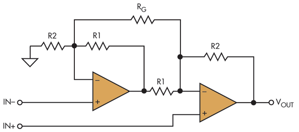
My primary candidates for the amplifier are the LMH6643, OPA2830, and OPA2301. Currently, I have selectable gains of 200, 300, and 800 via 1K resistors at R1 and ~200/300/800K at R2 along with a 10K trimmer at Rg. I'm using this IA to measure a voltage drop across a very small resistance (10's Milliohms) with 50-100mA current flowing through that resistance, and the whole thing is only a couple ohms above ground as far as common mode voltage is concerned.
What I am seeing is a wide variance between multiple samples of the same part. We can stick with the LMH6643 for this discussion, but I see the same with the OPA parts as well. Some of the parts have the "zero" level(when diff input is 0V) above ground and some other parts are not showing some of the smaller amplitude signals that my "Golden Amp" can. The golden amp is a sample that has the zero level very close to ground and is able to produce amplification of the smaller differential inputs created by the system.
The LMH6643 is supposed to be good for common mode input voltages down to Vs - 0.5V. But I thought I would try using a negative supply to see what happens. I moved just the negative supply pin (Pin 4) to an adjustable -1.2V to -3.3V supply hoping that it would "pull" the signal out of the ground for the "Low" reading amplifier, but instead it "lowered the water" revealing the zero input level at a voltage below ground. Here are plots of the three samples with the top being the golden sample the middle being the low-biased sample and the bottom being the high-biased sample. The left side plots show single rail operation (4.5V and Ground) and the right side is the same circuit with a -1.2V rail. Note that all other elements of the circuit are the same, and resistor R2 remains connected to the system's ground node for all three. These offsets are independent of gain, at least for gains of 200,300, and 800 as observed.

What parameters found in the data sheet would allow me to determine the full range of possible offsets so that I can attempt to design in some null-offset circuitry. I was hoping to use this part in a single supply design, but the existence of parts with the hidden negative offset would be an issue as the intended signal would get masked in the single supply implementation. Also this first diff to single ended stage gets fed into second single ended stage where the output offset error will get much larger, possibly even saturating the second stage. I'm hoping to at least be able to find a single supply part that does not have any negative output offset as I can then possibly create a dynamic null offset stage using a differencing stage with a sample and hold capacitor. Any help would be appreciated!


