This thread has been locked.

If you have a related question, please click the "Ask a related question" button in the top right corner. The newly created question will be automatically linked to this question.

OPA2134 buffer for Audio ADC PCM3168

Other Parts Discussed in Thread: PCM3168, OPA2134

Hi:

I've been using PCM3168 for some time, for audio applications...

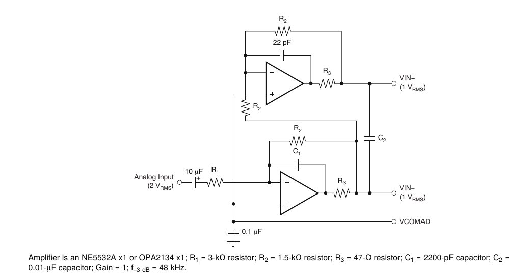
For the analog inputs i used the burffer shown in the datasheet:

I used it blindly cause what was important for me was making the codec work... but now i took a closer look...

Please correct me if im wrong:

The opamp of the bottom is just an inverter amplifier, with gain 0.5, and with a capacitor to cut waves above arround 48Khz... am i right?

Now the opamp of the top is another inverter amplifier with gain 0.5, whith it's input conected to the output of the first opamp... so combinign the two singals the total gain is 1 (0.5 in each differencial signal) and i have the desired differential output...

My question is... what is the 22pF capacitor of the top amplifier for? if the output of the first amplifier is already cut in 48kHz... wouldnt the output of the second be already cut at that frecuency? I know that the difference is not much, cause 22pF is just 1% of 2200pF, but shouldn't it work better without the 22pf capacitor? Or is something about the specific characteristic of this opamp what makes this necessary?

Thanks

  • Sorry... the gain of the top amplifier is 1 as the first signal is already multiplied by 0.5
  • Pablo,

    Most op amps cannot directly drive more than few hundred pF capacitive loads and in order to do so they require a Riso resistor to be added in series with the output terminal - see below.  However, this creates a problem of gain error when using a resistive load, RL, as the output is divided by the ratio of Riso and RL.

    To get around the gain error problem and still be able to improve capacitive load drive of the op amp, dual feedback configuration is employed - see below - similar to the configuration shown on your schematic.  For the AC input signal Cf acts like a short effectively placing the op amp in a follower configuration with Riso resistor improving the capacitive drive of the op amp.  The second feedback with Rf connect on the other side of Riso resistor providing the DC path to eliminate the DC gain error created by connecting resistive load, RL, at the output of the op amp with Riso resistor.

  • Thanks very much... And if i want to add a gain control to the buffer... could i just add a potenciometer with the middle to the input of the opamp and one side to the source? I left the other side unconnected... First i thought i should connect the other side to the output of the opamp...  with a 5k resistor i've got (simulating) a maximun amplification of 1.15 dB and attenuation of -122 (with a little variation for very low frecuencies)... With one side of the pot unconnected i get attenuation of -12 dB and amplification of 3.51 dB...

    I want to ask if i can do this configurations with this opamp or there is something of its characteristics that i'm not considering... as in the simulation (i use Qucs) i only have generic amplifiers (i will try with the spice model later on)

    This is the schematic:

    If The unconnected side of the pot is connected to the output of the amp i get the following maximun a minimun gain:

    Would you recommend me other configuration to add gain control to this buffer?

  • Pablo,

    Adding a resistor at the input wil work but only below cut-off frequency of the RC feedback network; above fc the gain will be ~1.  Please make sure to simulate the circuit to assure that you obtain the desired gain over frequency of interest.  BTW, I presume you use the dual supply for your application so that you do not violate the input common-mode voltage range.

  • Thanks for your help...
    Yes, i'm using dual supply of +/- 15V...
    I think my next step would be using the spice model of opa2134 to make a much mor realistic simulation...
    I've tried with the configurations stated in my previous post and worked in simulation for frecuencies till 500 kHz... only if i connect the pot after the Riso, the response starts going up...
    I think i will change the input resistor for one of 470 Ohms, and add a 5k Pot for controlling he gain... If i left unconnected one of the pot pins as i've shown in my previous post, i get a gain range of +9.5/-12.5 dB, which i think is good... I'm doing this because i don't really know which input voltage swing would i have for different instruments, so this way i could adjust the voltage swing of the output to match the codec... By the way, if my codec states that my analog input should be at most 2 Vrms... could i assume that that means that my signal should be less than sqrt(2)*2=2.83 Vpp? That is that the input of the codec should have a voltage swing smaller than 2.83V?
    I know that this conversion is only for sine waves... but i don't know how to calculate my allowed Vpp for audio... perhaps i should ask this in ADC forums...
    Thanks for everything
  • Pablo,
    You are correct that 2 Vrms in sinusoidal waveform translates into the amplitude of A=sqrt(2)*2V=2.83V but since such waveform can have opposite polarity (+/-2.83V), the total peak-to-peak voltage is 5.66V.
  • Thanks very much for your help!
  • Hi:

    It's has been a lot since i worked in this project, and everything worked fine... but i have one more question (perhaps it's a dumb one). In the schematic i posted in the first post, could someone tell me what is C2 for? I was told that it helped to keep differential signals in phase (i mean, that both corss zero level at same time), but i cannot find any theorical confirmation of that... If someone could explain it to me or give me some reference to look for it i woulw be very grateful.

    Thanks in advance.

  • Pablo,

    At higher frequency, C1 and C2 act as a short thus form buffer configurations that then allows R5 and R6 to isolate the capacitive load and by doing so stabilize the circuit.

  • Hello Pablo,

    The capacitor acts as a short at higher frequencies so the amplifier is in the Riso circuit configuration to help stabilize the amplifier. I recommend watching our TI Precision Lab videos on Stability.

    Thank you,

    Tim Claycomb

  • Hi:

    Thanks both for wour quick answers. But i think we are refering to different schematics... that explanations are about the feedback capacitors of the riso + dual feedback configuration, aren't they? Now i'm refering to C2 in the first schematic, the one that is between the outputs VIN+ and VIN-, C2 = 0.01uF. Perhaps i didn't explain myself correctly. Is that capacitor also for stabilization purpose?

    Thanks