This thread has been locked.

If you have a related question, please click the "Ask a related question" button in the top right corner. The newly created question will be automatically linked to this question.

OPA1S2384EVM

Other Parts Discussed in Thread: OPA1S2384, TINA-TI

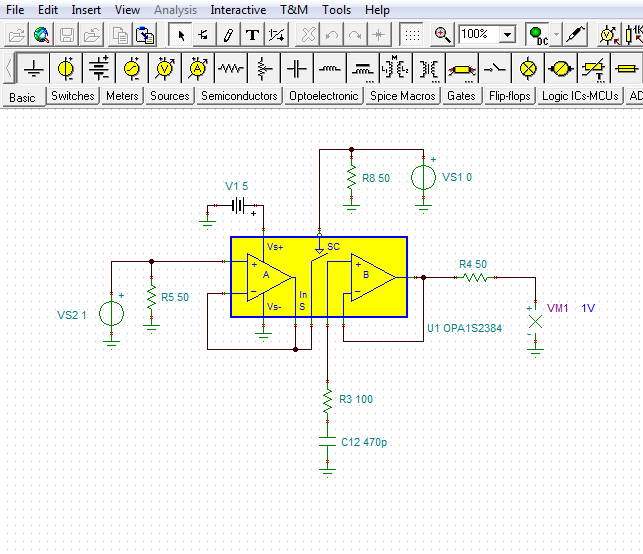
I bought opa1s2384 EVM and connected it to a Hamamtsu PMT H10721-20 and the light has sinusoidal modulation of 120MHz. We expect to see this light in this frequency but we have an output of CW signal approximately 0.6V. Before we checked the output of the PMT to the oscilloscope and saw a good sine signal of 120MHz.

  • Hello Leonid,

    The OPA1S2384 small-signal bandwidth runs from about 90 MHz to 250 MHz, depending on the gain and circuit configuration and passive components used around the amplifier. With an small input signal having a frequency of 120 MHz there should be enough amplifier bandwidth for sine wave to appear at the output. I wouldn't expect there to be much open-loop gain remaining at 120 MHz so the gain accuracy could be low.

    Looking over the OPA1S2384 EVM schematic it appears that as received by the user that some passive components are mounted on the PC board. R5, a 49.9 Ohm resistor is in right at the J2 input to ground. If it is in place on your board it will load your photo-diode sensor, in which case very little voltage would be developed across R5. R1 is a 0 Ohm resistor and that sets the gain of the first stage, A, to + 1 V/V.

    The switch control (SC) pin needs to be "high" or +2.4 V above V- for the switch to be closed. If the switch is open, then the signal won't be passed to the output amplifier "B."  

    The output amplifier, stage B, is set up wit a gain of +1 V/V too. If a large capacitance, cable or other, is connected after R4 the 49.9 Ohm resistor a low-pass filter is created. That would attenuate a signal that had been passed to the output. That probably wouldn't eliminate all traces of the signal, but would attenuate it. 

    There does need to be some positive dc input offset so that the output of the OPA1S2384 isn't forces against the negative supply rail (V-). The amplifier cannot amplify if the output is in saturation. The datasheet Electrical Characteristics table the output typically swings to about 100 mV from either supply rail.

    If you provide your OPA1S2384 circuit schematic set up on the EVM we should be able to review it.

    Regards, Thomas

    PA - Linear Applications Engineering

  • Hello Thomas,

    Below is a schematic of our circuit. We have the correct resistors at R5 and R4. The switch was closed during our measurements and we did not see a signal at TP1 either.

  • Hi Alec,

    The first thing I would do is test the OPA1S2348 EVM circuit an appropriate RF signal generator. Most RF signal generators are specified to drive a 50 Ohm load, and R5 connected across the J2 input would be ideal. Make sure a 50 Ohm coaxial cable is used to connect the generator output to the EVM J2 input. Also, most generators have a provision for adding a dc offset to the RF signal. That will be required to move the RF signal which will be centered about 0 V, to a positive dc level within the common-mode input range of the OPA1S2348. If you are using a 5 V supply for V+, setting the dc offset to +2.5 V places the zero-crossing of the RF signal right in the middle of the input range.

    Observe the output of the EVM with a wide-band oscilloscope, 300 MHz minimum. I would start out with a low RF frequency like 1 MHz, and make sure the signal is being seen with a gain of +1 V/V as expected, at the output J3. Then, increase the frequency until you either you see the output signal disappear, or reach the 120 MHz you wish to observe. If all of this goes well, then the EVM is not the issue.

    I reviewed the specifications on the Hammamatsu photosensor module that you are evaluating. It is specified as a Current Output Type Photosensor. The maximum output signal current is rated at 100 uA so the output current may be less than that at times. And in only one place on the datasheet does it mention a load impedance; 1 Meg in Specification Note 5. There are two issue I find:

    1. If the load impedance you are applying to its output is R5 (49.9 Ohm) at the EVM J2 input, the output current may be too low for any appreciable voltage to develop across the resistor. 
    2. If the module RF is centered about 0 V, and its output level is low, the output of the OPA1S2348 may be up against the its lower output rail. A dc offset at the input of the EVM would be needed to move the output off the rail.

    I hope these suggestions help you get it working.

    Regards, Thomas

    PA - Linear Applications Engineering

  • Hi Thomas,

    We tried applying a low-frequency signal with a frequency generator while measuring the output of the EVM with a wide-band oscilloscope. The result was the same CW signal which we observed with our PMT. 

  • Hi Alec,

    Have you made sure that the output is operating in the linear range, and its not against the negative supply rail? If the output is railed (saturated) you may not see any evidence of the input signal. What dc voltage levels do you measure at +IN A (pin 4), OUT A (pin 1), +IN B (pin 6) and OUT B (pin 8)? Also, trace the ac input signal at each of these pins.

    Regards, Thomas

    PA - Linear Applications Engineering

  • We are currently using single supply voltage. 

    We measured the following DC voltages at each pin:

    +IN A: 180mV, OUT A: 920mV, +IN B: 640mV, OUT B: 308mV

    The AC signal at each point was 0.

  • Hi Alec,

    It is difficult for me to know your exact setup conditions, but those voltages don't make much sense because the amplifier stages are set up as voltage followers having a gain of +1 V/V. If there isn't a voltage at the +IN A input it should be pulled down to 0 V, by R5. In that case, the output of the first amplifier section and the output of the second section should both be against the negative supply output rail when the switch is closed. Applying a dc level to the input should result in nearly the same voltage at the output of the second stage. Again, with the switch closed.

    I have set up your basic circuit in our TINA-TI simulator. It allows one to simulate your circuit and see what the output should be for a particular input. This may serve as an aid when you troubleshoot your circuit.

    If you don't have TINA-TI you can get it here:

    Regards, Thomas

    PA - Linear Applications Engineering

    OPA1S2384_test_01.TSC

  • Good morning Thomas,
    Would it be possible for you to give us an RMA# so we could send back the amplifier and you could test its functionality?
  • Hi Alec,

    I don't have the authority to issue an RMA from Applications Engineering. If the customer suspects a quality issue with the OPA1S2384 device, they make a request for a failure analysis though the distributor that supplied them the device. The distributor then provides them with a TI "Failure Analysis Request Form" which the customer will need to complete.

    The system that TI has in place is very complete and assures that the device is received by the right people, receives correct processing and is tracked through the TI quality system. The device will be thoroughly electrically tested as one of the first actions upon receipt of it.

    Regards, Thomas

    PA - Linear Applications Engineering