This thread has been locked.

If you have a related question, please click the "Ask a related question" button in the top right corner. The newly created question will be automatically linked to this question.

Unknown wave with the OPA846

Other Parts Discussed in Thread: OPA846, TINA-TI, OPA354

Hi guys


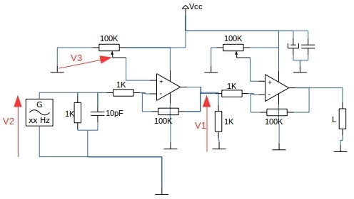
I'm trying to make a high gain amplifier which consists in two stages of 40dB each (x100). I'm using the OPA846 which should fulfill the gain requirements for at least 1 MHz bandwidth. The voltage input would be very low like 2 mV and would have offset, so it has to be compensated and that's why the positive input has a variable voltage reference.

The schematic is in the next image: By the way Vcc is 5V:

V1 should be the result of combining the two sources (correct me if I'm wrong), the input and the reference. V1 = 101 · V3 - 100 · V2 = 100 · ( 1.01 · V3 - V2 ) ~ 100 · ( V3 - V2 )

I've tested it with an oscilloscope probe and the results are in the next two images (sorry, I only have a two channel oscilloscope):

The screeshots were measured with 16 samples averaging to lower the noise.

Let's start with the second oscilloscope image, this screeshot shows the input (V2 in yellow) and the voltage reference in the positive input of the first stage (V3 in blue). As you see there is a little crosstalk in V3 which I don't know if would affect the proper behavior of the amp. The voltage reference is a lot greater than the input voltage, if I lower the reference a bit the output goes to zero and if I increase it the amp saturates to Vcc. Also the math channel (in red) shows V3-V2 which is the signal that the amp should amplify.

The first screenshot shows the input (V2 in yellow) and the output of the first stage (V1 in blue). The output should be the signal in red from the second image multiplied by 100 but it isn't.

Well, I'm a bit lost with that, could anybody explain what's happening?

Thank you in advance, by the way have a nice weekend.

  • Hello,

    Is your question about the sawtooth wafeform, or the offset voltage?


    Gain bandwidth product refers to small signal bandwidth.  Large signal bandwidh is more correlated to slew rate.  The signal in the first scope trace looks like a slew limited signal. 

    What is the frequency of the square wave?  What kind of scope probe are you using?  Do you know how much capacitance the scope probe has?   

    Regards,

    Loren

  • Hello Loren,

    First of all, thank you for being interested in my question.


    My question is about the waveform itself but also the offset. You said that the slew rate is limiting the output, as you could see, the input signal that should be amplified (V3-V2) is showed in red in the oscilloscope screenshot. That signal is about 100 mV peak to peak and has an offset of 460 mV more or less, since the gain is set to x100 the output should be 10 V peak to peak and 46 V offset which is not possible and the output should be saturated to +Vcc. Am I wrong?

    The square wave has a frequency of 1000 Hz, the scope probe is a Tektronix TPP0201 which has a 1 MΩ/20 pF  input.

    Kind regards,

    Daniel

  • Hi Daniel,


    Have you tried simulating this circuit in TINA-TI.  Do you want the device to saturate? 

    I am still not clear on your question. 

    Regards,
    Loren

  • Hi Loren,

    I was using the OPA846 with single supply (+5Vdc) because the development requires it, the OPA846 is not suited for that kind of supply so I switch to OPA354. I think the strange waveforms were caused for that reason.

    I've found TINA very useful and very powerful, thank you for the advise.

    Regards,

    Daniel.