This thread has been locked.

If you have a related question, please click the "Ask a related question" button in the top right corner. The newly created question will be automatically linked to this question.

LM358/LM358-N Question

Other Parts Discussed in Thread: LM358, LM2902, LM324, LM2904, LM358-N, LMV324

Hi,

Let me ask you a basic question about LM358 application circuit as below.

Is a load resister like "Rb" (6.2K ohm) necessary to use LM358?

What is the purpose of this load?

Thank you for your support. 

  • Hello Takumi,

    See the second paragraph of section 7.4 in the Apps section.

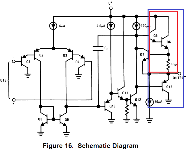
    "To reduce the power supply drain, the amplifiers have a class A output stage for small signal levels which converts to class B in a large signal mode. This allows the amplifiers to both source and sink large output currents. Therefore both NPN and PNP external current boost transistors can be used to extend the power capability of the basic amplifiers. The output voltage needs to raise approximately 1 diode drop above ground to bias the on-chip vertical PNP transistor for output current sinking applications.

    For ac applications, where the load is capacitively coupled to the output of the amplifier, a resistor should be used, from the output of the amplifier to ground to increase the class A bias current and prevent crossover distortion.

    Where the load is directly coupled, as in DC applications, there is no crossover distortion."

    This "feature" is unique to the 30V LM358 and LM324 (and LM2902 and LM2904) family. The low voltage LMV3xx versions have a conventional output stage and do not require a pull down.

    If you use another amplifier in the above circuit, a pull down is not required.

    Regards,

  • Hi Paul-san,

    Thank you for your reply!

    You mean the datasheet section "7.3 Feature Description", right?

    http://www.ti.com/lit/ds/snosbt3i/snosbt3i.pdf

    And let me ask you following qestions again please?

    Q1) A 6.2Kohm resister is used on the circuit of Fig40/41.

    Will you tell me how to calculate the value of the resister?

    Q2) Internal circuit

    According to the datasheet, LM358-N works as A-class amp in case of small signal and in case of large signal it works as class-B.

    Fig 16 is internal circuit. I think "Red" I marked is A-class and "Blue" is B-class. Is this correct?

    A extra resister is needed to vias "A-class" amp, right?

    About small signal and large signal, what amplitude(voltage) is threshold?

    I do not understand well the behavior of this output stage.

    I suppose, as the changing timing from Class-A to Class-B is not very good, sometimes low side PNP transister remains off. 

    How is my idea?

    Q3) Internal circuit value

    I think I would like to simulate this internal circuit.

    Would you tell me the specifiation of NPN/PNP transister and resister value?

    Q4) Recommend OPamp

    Could you recommend me another OPamp instead of LM358-N, if possible?

    Sorry for my poor question...

  • Hello Takumi-san,

    The LM324 was originally designed to drive resistive loads returned to ground (V-).

    You are correct - the red is the "class A" circuit, or the sourcing stage. It does not change to AB (blue) until the output is about 1V above GND and Q13 can fully bias. Look at the output sinking current graph (figure 11), notice it has a "knee" in it between 30-80uA.

    You need to source at least 50uA from the output to reduce the crossover distortion. The more current drawn, the less distortion, but at the cost of positive output swing (and possibly increasing distortion due to loading the output too much).

    The schematic is a very simplified schematic. The actual transistor parameters are proprietary - but the basic operation can be modeled with a few generic low power PNP transistors (2N3906). I believe Rsc is 30 ohms.

    If you are using the LM324, I can only assume you are using it because of the price. There are other many replacements that do not have this "feature" on the output.

    If your supply voltage is 2.7 to 5V, then you can use the LMV324, which is the low voltage version, but has a conventional R-R output and DOES NOT have the output glitch. If your supply votlage is greater than 5V, then there many replacements and you will need to specify your requirements (supply voltage, package, BW, price...).

    Regards,

  • Hi Paul-san,

    In fact, I have still been struggling to understand this OP Amp well... (^^;

    Would you support me with my basic questions?

    Q1) Output stage transistor

    I understood that

      Q5+Q6 : Darlington transistor

      Q7 : Positive Output buffer(driver)--A class

      Q13 : Negative Output buffer---B class

    Is my understanding correct?

    Q2) PNP transister "Q13" movement

    I do not understand well about the behavior of Q13.

    Q13 does not work(active) until the output voltage is over 1V.

    That is to say, the output swing can not be under 1V.

    As a result, the output range of negative side is from 1V to 2.5V in case of Vcc=5V, I think.

    But the specification of the min output is 20mV(Max). (datasheet page 8)

    I do not understand well the relation between output swing and Q13 behavior and fig11("knee") graph.

    Q3) Bias resister

    There is an explanation datasheet page 12 as below.

    I do not understand well this explanation.

    We need to use resistor in case of "capacitive" load and need not to use in case of resistive load?

    And in case DC application, we need not to use resistor to bias, correct?

    And you said that "You need to source at least 50uA from the output to reduce the crossover distortion.".

    Why 50uA? Could you tell me how to calculate?

    I do not understand well why this resister works for" bias" of "Q7".  

    Q4) Rsc

    The Rsc(30ohm) of output stage is bias resistor for Q7, right?

    Q5) LM358-N vs LM358

    What is the difference bewteen LM358-N(NS) and LM358(TI)?

    I think both are very similar but there is no discription about "bias" resistor on TI.

    About LM358, we do not need to use "bias" resister to prevent crossover?

    I'm very sorry for my too basic question.

    Probably, due to I do not undrstand well the behavior of transisitor...

    Best Regards,  

  • Hi Paul-san,

    Though it takes long time (around 4 months !!), I think I could understand the internal circuits of LM358.

    Sorry for my too basic questions...

    But I do not understand one point, that is "6uA"  current source at the input stage and buffer stage.

    Probably "6uA" is from "slew rate" of LM358, 0.3V/uS.

    Is my idea correct? But I suppose it seems to be good its current is 10uA, for example...

    If you have the information, please let me know.

    Thanks!