This thread has been locked.

If you have a related question, please click the "Ask a related question" button in the top right corner. The newly created question will be automatically linked to this question.

Wide Bandwidth Optical Front-end Reference Design - TIDA-00725 .

Other Parts Discussed in Thread: OPA857, THS4541, TIDA-00725, TIDA-00978, ADC34J45, ADC32J45

hello to everyone,

I am currently using a fast transipendance amplifier based on OPA857 (20KOhm gain setting) and an Hamamatsu PIN diode S5973 0.8pF@5V. I think that, between other problems, the connection from the PD to the OPA857 has  too much capacitance preventing expected bandwith results and increasing the noise. I note that I will also benefit with an extra gain, a factor 10 will be more than enough.
For this reason, I was looking for a more integrated and performant solution. I have seen that you demonstrate an Optical front end with OPA857 and THS4541, the TIDA-00725.

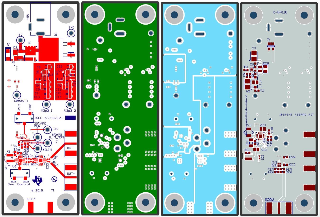
Now, TI authors have added the designs, BOM PCB and the schematics for the signal chain circuit and laser diode source circuit in the files tidcbf1.zip and tidcbf2.zip. Very good, very useful for me, but I see that Gerber files contained in the tidcbf1.zip and tidcbf2.zip are sometimes duplicated copies of one design and are missing intermediated layer says, layer 2 and 3. Is it possible?

where I will found the files for the 4 layers

thank you very much

  • I am here again:
    I add some other information that may help:

    I have no experience at all about PCB intreagtion at this small scale components size and at such high frequency. That is why I would like to use a proven circuit.

    Seconldy, I have not the possibility to realize directly the four layers PCB but only 2 layer with LPKF laser machine of the electric workshop. Anyway I could ask for express service around. could you suggest me a valid provider of 4 layer PCB even populated?
    I have not seen the TIDA-00725 as evaluation-board to buy. Is it possible to acquire it, even only the PCB?

    tird, In the TIDA-00725 there are also the power regulators and a tird party high voltage supply for Avalanche photodiode, that I do not need. These all complicate the circuit. I add that I have already the ultra low nois regulators at 3.3V and 5V that I can use, <1uV and projected for high freq application. I could use them bypassing with capacitor near the OPA857 and the differential THS4541. Could it help?

    thank you very much in advance for any support.
    Andrea
  • Hello Andrea,

    I will ask the circuit designer to look into this.

    Regareds,
    Loren
  • Hello Andrea,
    I am not sure what you are referring to in the layer images above. It does have all 4 layers. Also, I looked into the gerber files and it looks like all 4 layers are in there. The 4th layer is shown as the "Bottom Layer". The 1st layer is the "Top Layer". Can you please be more specific on what is repeated.

    Where are you located? In the US we have a variety of vendors that can manufacture 4 layer boards. We use Advanced Circuits, Krypton and Sierra Circuits as a few examples. I am not sure what you have around where you are located.

    If it is simple enough you could try and design the board on just two layers. Since you will using simple regulators and power supplies, the design may be simple enough to do on 2 layers. However since this is a high-speed design you should try and maintain the 2nd layer as a GND plane. Unfortunately we are not currently selling the PCB used for this design. A linear regulator with appropriate bypassing should be sufficient for the design. You only need the APD supply that I used in case your APD needs to be biased to > 10V.

    -Samir
  • Dear Loren thank you very much for the support.
    Dear Samir, thank you very much too.
    Probably it is my fault because i have not much experience, I see correctly top and bottom layers .GTL and .GBL in the design files TIDA-00725 Gerber (TIA OPA857 THS4541) . . There all the files, inside the zip, are named like
    TIDA-00725_TIA_OPA857_THS4541_Gerbers/GerberNCdrills/6590370A.*.* but nothing is like the green and cyan images in the picture I reported above (I take them from your pdf). which software you suggest to open the gerber file?

    I am currently a researcher in plasmonic in a University lab at KAUST in Saudi Arabia and I come from Italy. Practically, at my knoledge, there is no one that can supply 4layers PCB service here around :(
    If necessary I will contact one of those you haved suggested, thank you very much!

    Here in LKAUST we have an electronic workshop that produces routinely simple PCB and custom circuits. If you think I can try 2 layers solution it would be much faster and direct for me, they have also a LPKF ProtoMat S103 for RF circuit. I have with me some Roger PCB 2 layer laminate serie 4000, that should works fine for high frequency application. You suggest to maintain the GND on the second layer, it means that 3.3V supply and signal will be on the top one?, should i have to plan any guard ring near the input of my PIN photodiode?

    I add that i do not need an APD because I can rise up the optical signal up to max 500uW a 80Mhz sinusoidal carrier signal at my convenience that I think is at the limit of the output swing of OPA857 even at 5K gain. (normally I use ten or few tens of uWatt, that is why I appreciate the extra 5X factor introduced with the THS4541.

    thank you very much for your support!
  • I have also other two questions:
    1) I use high frequency carrier and Lock in detection since the physycal signal is a decade lower in frequency. I have seen that you suggest to filter the signal to improve the SNR with a lowpass 3-order Bessel filter . Do you think it will be equally useful to use a passband 3order around 80Mhz +/-7 Mhz -3dB ?

    2) what about the thickes of the metal layer and interleave layer in the 4 layerPCB? is it stringent the 15-20-15-...mill or something similar will be equally well?

    thank you very much again
  • Hi Andrea,

      The color pictures were extracted using altium designer. That is just a PCB layout image extraction that comes as part of the tool. There are some free gerb tool viewers available online. Advanced circuits looks like they have a 3rd party tool shown below:

    If you have GND on the bottom layer then signals and power will have to be routed on the top layer. I think the design is simple enough in this case so hopefully its pretty straightforward. I don't think a guard ring is needed. I have used guard rings in the past when working with very low current levels....pico-amps. I haven't really had to do a high-speed and low current level application.

    How do you plan on observing the differential analog output of the THS4541. Do you have an ADC or a differential scope probe? What kind of end application/system are you working on?

    -Samir

  • Dear Samir,

    thank you again!

    "The color pictures were extracted using altium designer." Now I understand. So you confirm me that in your gerber version of the file there are all the 4 layers. I will try to open it with the gerber viewer you suggested vi Advanced Circuits. Thank you.

    In case I will try a 2 layers I will follow your suggestion: GND bottom layer, signal and power on the top, no guard ring. (I will have minimum tens of nano-amps to  tens of micro-amps carrier wave modulated about 50% by the signal, but I can rise more the signal reducing a bit the full-scale).

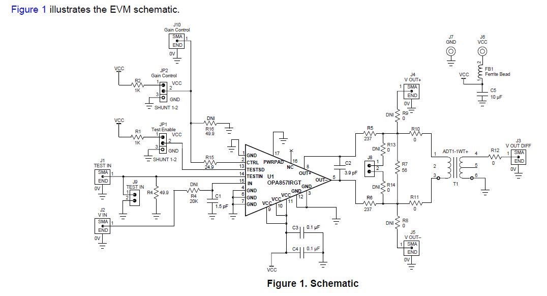
    About the differential analog output of the THS4541, I plan to use the same solution you propose in the evaluation board for the OPA857 , to use a minicircuit transformer, the ADT1-1WT to convert in single ended, Is it possible? can you suggest something better? 

    (I have the EVM OPA857 that use this solution).

    In lab we have also differential front end for FPGA acquisition board.

    My final application is a basically to improve the capability of a  positioning system that track relative position, at the nanoscale,  of plasmonic structures I use for

    current sensing and spectroscopy with few nm resolution. Dynamic information enters in when I stress elastically/plastically  the sample with piezo shacking or via thermal photo-elastic effect.

    Actually I can access some hundreds of KHz, not more.

    Today I was

    About

  • ops...

    Today I was comparing OPA857 datasheet with others, and I realized that now on the site there is a new TI Designs "Reference Design for Extending OPA857 Transimpedance Bandwidth" TIDUBX71–April 2016, TIDA-00978. It is your. Interesting !!

    I would like to go back to the TIDA-00725
    I have a question about the noise measurement you have performed and the integrated noise data you have reported:
    365 μVRMS and 840 μVRMS for the 5-kΩ and 20-kΩ transimpedance-gain settings
    NR7500 + OPA857 (G = 5 kΩ) + THS4541 + ADC34J45 = 525μVRMS
    NR7500 + OPA857 (G = 20 kΩ) + THS4541 + ADC34J45 = 1300μVRMS
    all these noise are uncorrelated , they can be obtained one from the other via the squared sum of each single term
    These are obtained with no optical signal applied, is it?
    Have you measured also the noise including the optical source?
    My lock-in application, with time-constant about 10 cycles, would works as averaging the signals improving the SNR, is it correct?

    thank you again Samir for your support.

    Regards, Andrea
  • Andrea,
    You can certainly use a transformer to convert the differential output to single-ended, however you will lose any dc effect because of the transformer. As long as the bandwidth of the transformer meets your requirements you should be okay.

    In my design I used a high speed ADC32J45 to digitize the output of the THS4541 so I was able to preserve the dc content of my signal.

    -Samir
  • Andrea,
    The noise is uncorrelated so it should be the square root of sum of squares. I disconnected the fiber from the laser source to the photodiode during these tests since I wanted to quantify the noise of just the receive (Rx) signal chain. I haven't measured the noise of the system with the optical source connected.

    You are correct, the system SNR will reduce with averaging. For the OTDR application I was able to use > 10k averaging to bring the noise down to the tens of uV level.

    -Samir
  • Dear Samir,

    thank you for your comments. I am still not decided about to use AC or DC coupling.

    I have a instrument controller , the R9 (RHK), that I will use for my setup. It has  fast lock-in (250MHz), and direct analog signal inputs up to 20MHz that accept single ended or differential signals.

    I have considered your solution with the ADC32j45. 

    next day I will organize ideas to realize a 2 layer PCB. I will need 3 or four of such front end.

    Thank you again.

    Andrea