This thread has been locked.

If you have a related question, please click the "Ask a related question" button in the top right corner. The newly created question will be automatically linked to this question.

TLV3202 Issue

Other Parts Discussed in Thread: TLV3202, LM2904, LM2903, TLV3201, LMV7272

Hi Team:

My customer use below circuit.

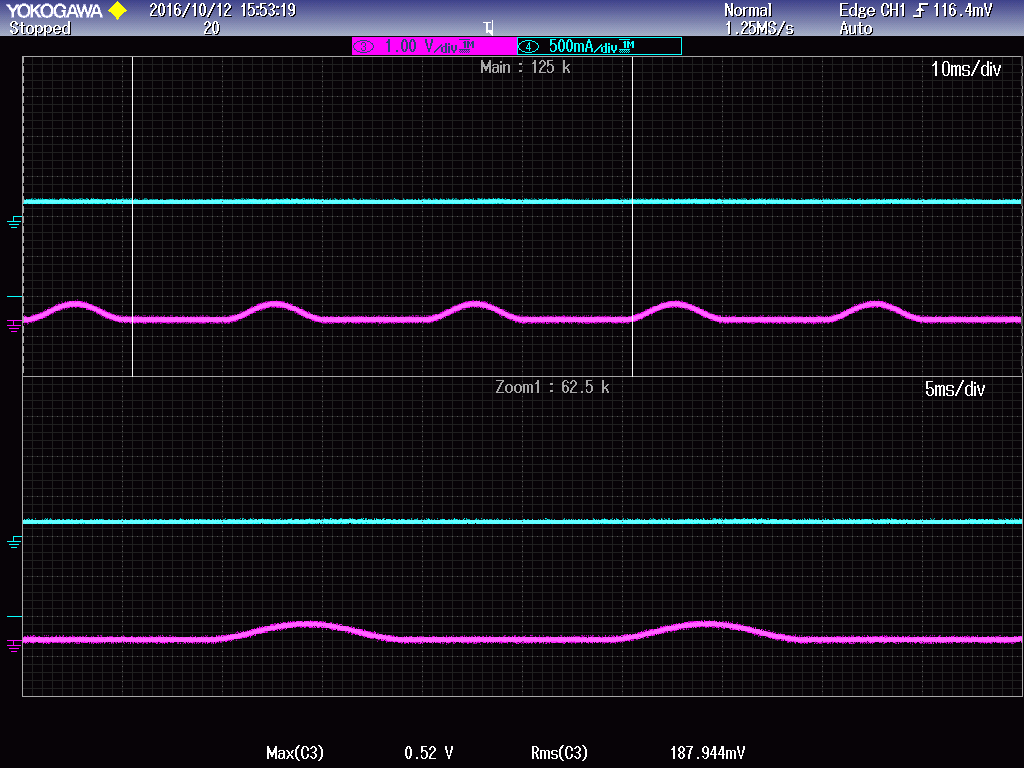
U145 if they use TLV3202, the DAO1(Comparator input pin) will be like below:

If they replace the TLV3202 with LM2904, the output will be OK.

And they try to modify the input sigal with 100mV.

They find the input pin will be like this :

Could you give me some idea? Why will be like this?

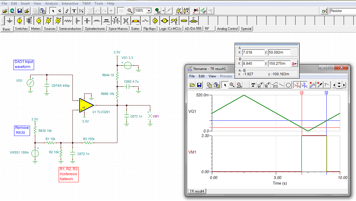
And we have remove IN+ AND IN- pin external components, the IN1+ pin only connect the 100mV power supply, IN1- only connect the DAO1

  • Hello Derek,

    I believe the differences observed in the output responses for the LM2903 and TLV3202 are due to the TLV3202 being a much faster comparator. It appears from the images, especially the third one, that the TLV3201 is switching output state very rapidly when the two input voltage levels are close to equal in value. When they are approximately equal and being compared any noise riding on one and/or the other, will result in the comparator flipping state as one level momentarily exceeds or drops relative to the other. What results is a burst-like output that occurs until the two input levels are separate far enough from each other such that the noise riding on them stops causing the output to change state. The TLV3202 has response time (propagation delay time) around 45 ns, compared to about 1 us for the LM2903. The TLV3202 can switch state many times in the same time period as the LM2903 switches once.  

    Very often hysteresis is applied to comparator circuits to reduce their noise sensitivity. It is a form of positive feedback that establishes two different threshold levels unique for the up-going and down-going voltage transitions at the inputs. There is a lot of information on-line about adding hysteresis to comparators. The TLV3202 datasheet discusses hysteresis in the External Hysteresis section on Page 9. Another good TI resource on the subject is the Application Notes section of the LMV7272 comparator datasheet. I do think that adding hysteresis to this circuit will help eliminate the behavior.

    Regards, Thomas

    PA - Linear Applications Engineering

  • Thomas:

    Thanks for your reply. It's helpful to me. I will try to add hysteresis.

  • Thomas:
    One more question, the LMV7272's datasheet show how to add hysteresis for stable reference.
    But in real application my customer's reference is output from the FPGA, it's a triangle wave.
    How to add hysteresis?
  • Hi Derek,

    There are a couple of questions I need answered before we get to adding hysteresis to the TLV3202 comparator circuit.

    1. Are R627 abd R633 76 Ohms as it appears to be on the schematic? If so, the voltage level on 1IN+ and 2IN+ are only 24.8 mV above ground.
    2. Is the label VADCI- connected to ground?
    3. It appears that A_PV+ is ac coupled to inputs 1IN- and 2IN- via C676/R631 (2.2 nF/30.1 k) and C681/R35, respectively. What is voltage A_PV+?
    4. Also, it appears that DAO1 and DAO2 each drive 1IN- and 2IN- directly. What is the level (pk-to-pk + dc), frequency and expected waveform type?
    5. How much hysteresis would you like to apply? Remember that the 1IN+ and 2IN+ inputs appear to be operating very close to ground so the amount of hysteresis that can be added will be limited to a few tens-of-millivolts at most.

    Regards, Thomas

    PA - Linear Applications Engineering

  • Hi Thomas:

    1. R627 and R633 is not on the board. They are NULL (Described in the schematic). They add 100mV offset at the HSS1.

    2. VADCI is real ground.

    3. They have removed the C676/R631 and C681/R35, it means A_PV+ source is also removed.

    4. DAO1 and DAO2 is the wave which I post firstly.

    The range is about 0 - 800mV.

    5. 100mV is enough. They add 100mV offset at that pin.

  • Hi Derek,

    I set the TLV3202 up for 100 mV of hysteresis relative to the VHSS1 100 mV dc level. I drew one-half of the comparator circuit in TINA using the original schematic as a basis and then incoporating your latest notes about the circuit setup.

    You can see from the TINA diagram seen below that the circuit is producing just about 100.2 mV of hysteresis. I hadn't ever applied hysteresis to a comparator operating with the inputs so close to the negative supply rail and things were worked out a little different than when it was applied near mid-scale. Nonetheless, I found a solution. This should work as needed and provide a lot of noise immunity. Note that since VHSS1 is applied to the non-inverting input network that R630 shouldn't be needed. Also, I would add a 100 nF power supply decoupling capacitor right from the TLV3202 Vcc pin to ground.

    Regards, Thomas

    PA - Linear Applications Engineering

  • Thomas:
    Great thanks for yoru support.
    Could you let me know how to get this register value?
  • One more question. TLV3202 is a push-pull comparator, it still need add Pull up circuit? Or add hysteresis must add pull up?
  • Hi Derek,

    I determined the hysteresis resistors using a slide from my TI Tech Day presentation, "Effective Application of Analog Comparators." The hystereis is applied to a comparator operating in an inverting mode, which is the mode the customer's circuit operates in. You can see the circuit and equations in the slide exhibited below.

    One difference that I observed between the circuit in the silde and the customer's circuit is the voltage applied to R1 is equal to Vcc,+3.3 V, in the slide and only +100 mV in the customer circuit. I found when I went through the calculations using +100 mV for the voltage applied to R1 that the 100 mV hysteresis (Vref+/- 50 mV) was correct, but the reference voltage I was shooting for, +100 mV, was about +50 mV high when I ran a TINA simulation. Analysis revealled that when the voltage applied to R1 was different than Vcc that an offset is introduced into the reference voltage. The amount depends on the various setup conditions.

    I have continued analyzing why this is occurring, but found that by simply moving the Vref down by -50 mV, to +50 mV, the hysteresis low voltage level is +50 mV and the hysteresis high voltage level is +150 mV, both centered about +100 mV (Vref +/-50 mV). The resulting R1 - R3 values are what I reported in my previous response.

    And yes, since the TLV3202 has push-pull outputs it does not need the R666 and R667 pull-up resistors.

    Regards, Thomas

    PA - Linear Applications Engineering