Other Parts Discussed in Thread: INA301, INA202
dear supporting team,
my customer is using INA201 in overflow protection circuit, the Rs is 0.67mOhm, and the overflow current threshold is 25A. the sch is as below, they want to know which spec of INA201 cause the issue and how to solve it.
R92 & R93 =100 Ohm,C77 1000pf,R88 5.11k,R89 2.26k,

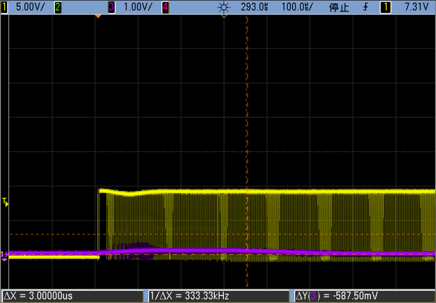
they found some INA201 sample will has mis-trigger when there is no loading(no input current), i.e. PIN3 will have higher than 0.6V voltage when there is no input. and also could not recover. the plot is as below:
failed chip: PIN3 output (purple curve)

normal one:
if remove R89, test PIN2 output when first powering up, when there is no current input, Vcm=5.6V, the waveform is as below:
yellow curve:power module output voltage, green curve:normal ina201 PIN2,purple curve:4.5v power supply of INA201,The blue curve is the failed chip PIN2.

if shut down the module, they will find during the power module output voltage decreasing (no current at Rs), OUT voltage will increase, and for normal chip and failed chip, the have big difference, so which character cause the difference? and how to revise their circuit to handle the problem?
yellow: output voltage of the module. green: pin2 of INA201. purple: power supply of INA201
failed chip:
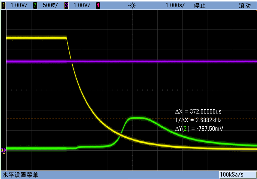
normal chip:

tks a lot!