This thread has been locked.

If you have a related question, please click the "Ask a related question" button in the top right corner. The newly created question will be automatically linked to this question.

TINA/Spice/LMH6551Q-Q1: ADC interface front end simulation

Expert 1730 points
Part Number: LMH6551Q-Q1
Other Parts Discussed in Thread: TINA-TI, , THS4509, ADS42LB69, LMH6551, LMH6518

Tool/software: TINA-TI or Spice Models

Hello,

       I need to interface a +/-5V (10Vp2p) signal to an ADC having an input range of 2Vp2p with a common mode voltage of 0.9V. 

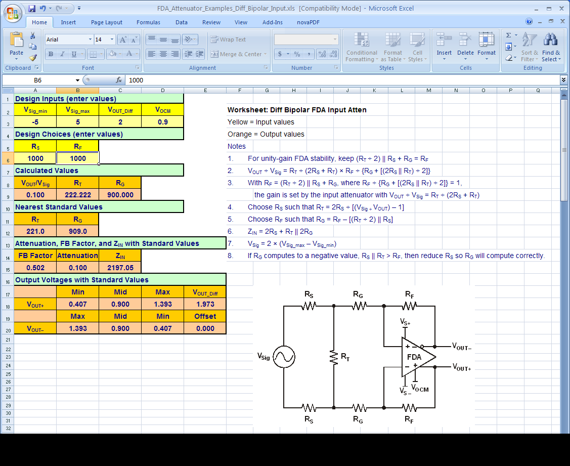
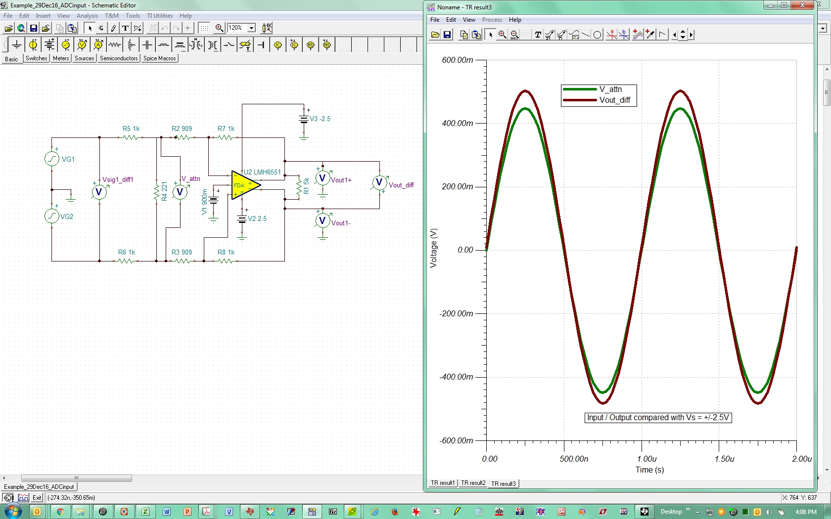
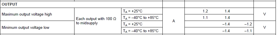
I chose the value for the different resistors (reference designators can be seen in the attached screenshot of the excel file; this excel file came with slyt336 application note from TI). 

To verbalize the setup:

1) Vcm of the FDA is set to 0.9V

2) V+ to 5V (although I suppose 2.5V is sufficient, am I right?)

3) V- to GNC (since the output only needs to have a positive swing)

4) The resistor values are Rf = 1K, Rg = 909E, Rt = 221E, Rs = 1K. 

Attached is the TINA schematic/simulation setup and following is the schematic screenshot

There are three questions:

1) I don't see the swing range as shown by the excel file

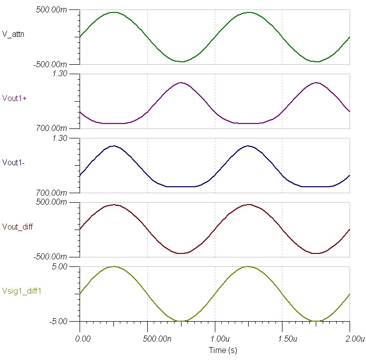
2) Vout+ & Vout- are distorted but their difference "seems" correct. Is this supposed to happen and is it correct to implement?

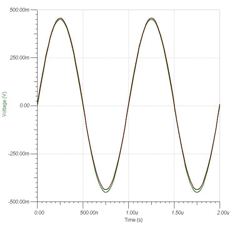
3) Vout_diff voltmeter is inverted in-order to see if the input and output waveforms are similar. It can be seen that there is a small dc-offset introduced in the output. 

 1205.Example_29Dec16_ADCinput.TSC

Thank you for your time in answering my questions,

Regards.

  • Hi SM,

    The LMH6551Q-Q1 cannot be used with a single 5V supply as you've connected it and be able to support your needs:

    VoCM= 0.9V

    Vout= 2Vpp diff.

    Each output would have to swing 1Vpp with Vocm set to 0.9V meaning minimum output swing is only 0.4V from ground. The datasheet shows that with 5V single supply (Vs= +/-2.5V), output swing is typically 1.1V from either supply rail (headroom = 2.5V - 2.8Vpp/2 = 1.1V):

    So, you would need to tie the V- pin of the FDA to a potential at least 1.1V below the expected minimum output swing (0.4V with respect to ground). So, either V- of -2.5V or -5V would work.

    Here is the response with Vs= +/-2.V where the swing looks "symmetrical" (but at a gain of >1):

    Here is the modified TINA-TI file for reference:

    LMH6551Q-Q1 E2E Question 12_29_16.TSC

    I could not find the Excel file you were showing and working with. If the swing does not match the spreadsheet prediction, please look to see maybe that calculator is setup for a FDA with Rail-to-Rail output swing?

    Regards,

    Hooman

  • Hello Hooman,

                  Each output would have to swing 1Vpp with Vocm set to 0.9V meaning minimum output swing is only 0.4V from ground. The datasheet shows that with 5V single supply (Vs= +/-2.5V), output swing is typically 1.1V from either supply rail (headroom = 2.5V - 2.8Vpp/2 = 1.1V):

    I couldn't have figured this out on my own!

    Following is the excel file that I got from TI

    FDA_Attenuator_Examples_Diff_Bipolar_Input.xls

    Some more questions: 

    0) Is 0.9V in the acceptable output common mode range of the opamp? As per a line in the same table of the datasheet, [min, max]|VoCM = [1.2, 3.8]. 

    1) As per the excel file, for the chosen resistor values the output swing should be 2V p2p, however we are seeing something closer to 1V p2p. May I ask you to please help me understand the difference.

    2) How can I know if the chosen values will lead to a stable design? 

    3) Introducing a negative voltage rail is always an issue, may I ask you to please suggest an alternate low cost FDA. The input signal BW is only 3MHz (max). 

    4) For another design we will be using the THS4509 interfaced to a ADS42LB69 (ADC). The ADC has VCM = 1.9V and input of 2Vp2p. We are planning to use this in a single supply configuration (+5V/0). Will this be ok?

    Vcm = 1.9V  & 2Vp2p => Max out = 1.9 + 0.5 = 2.4V and min = 1.9-0.5 = 1.4V. 

    May I ask you to please help me decipher the output voltage swing range possible for the THS4509 in single ended configuration from the datasheet. Unlike the LMH6551Q's datasheet, the THS4509 does not have any table for single supply operation. 

    5) Also for the THS4509 ckt, I calculated the acceptable common mode range for Vs+/Vs- = +5/0 as [1.1 3.9]. Is this correct? Then the VoCM of 1.9 (as required by ADS42LB69) should be ok, right?

    Thank you again,

    SM.


  • Hi SM,

    My responses below:

    Question 0) Is 0.9V in the acceptable output common mode range of the opamp? As per a line in the same table of the datasheet, [min, max]|VoCM = [1.2, 3.8].

    Response: You are talking about CMVR spec (page 5) when using Vs=5V (single supply). Again,the way to look at this is with respect to each supply rail (1.2V headroom from each supply). So, if you run your device from +/-2.5V, 0.9V would not be an issue (> 1.2V headroom from -2.5V). However, you would not be able to run it with single 5V supply at 0.9V CM voltage.

    Question 1) As per the excel file, for the chosen resistor values the output swing should be 2V p2p, however we are seeing something closer to 1V p2p. May I ask you to please help me understand the difference.

    Response: I think that spreadsheet is based on computation only and does not take into account the device limitations.

    If I were to do what you want accomplished, I'd run the FDA with a gain close to 0dB and do the attenuation on the front using a matching attenuator such as this one:

    You get the following design if I use 50ohm source impedance and plug in 14dB attenuation (10Vpp to 2Vpp is -14dB):

    Here is the TINA-TI for the circuit above for reference:

    LMH6551Q-Q1 14dB front attenuation E2E Question 12_30_16.TSC

    Question 2) How can I know if the chosen values will lead to a stable design?

    Response: TINA-TI is pretty good at prediction instability. Do Transient response for a step input and monitor the ringing.

    Question 3) Introducing a negative voltage rail is always an issue, may I ask you to please suggest an alternate low cost FDA. The input signal BW is only 3MHz (max). 

    Response: You can take a look at RR output FDA's here which I've already filtered for your needs:

    Question 4) For another design we will be using the THS4509 interfaced to a ADS42LB69 (ADC). The ADC has VCM = 1.9V and input of 2Vp2p. We are planning to use this in a single supply configuration (+5V/0). Will this be ok?

    Vcm = 1.9V  & 2Vp2p => Max out = 1.9 + 0.5 = 2.4V and min = 1.9-0.5 = 1.4V.

    May I ask you to please help me decipher the output voltage swing range possible for the THS4509 in single ended configuration from the datasheet. Unlike the LMH6551Q's datasheet, the THS4509 does not have any table for single supply operation. 

    Response: With the THS4509, you'd need 1.4V (over temp limit) headroom to either rail (comes from Min / Max output voltage, page 7, of +/-1.1V with Vs=+/-2.5V). So, you'd be "barely" ok with the conditions you've specified as you are just on the hairy-edge with 1.4V minimum swing!

    Question 5) Also for the THS4509 ckt, I calculated the acceptable common mode range for Vs+/Vs- = +5/0 as [1.1 3.9]. Is this correct? Then the VoCM of 1.9 (as required by ADS42LB69) should be ok, right?

    Response: I disagree. With 3.9V CM voltage. The maximum swing (=3.9+0.5=4.4V) gets you within 0.6V of 5V for the V+ supply which is too close! From Response 4 above, you must observe the 1.4V headroom to either rail which limits your highest CM voltage to 3.1V. For the minimum CM voltage, you are looking at 1.9V minimum CM voltage placing you on the edge of CM minimum.

    Regards,

    Hooman

  • Sorry!

    Looks like the FDA selection tool link I sent you for Response 3 above, does not include the filters I imposed. Here is the screen shot:

    Regards,

    Hooman

  • Hi SM,

    I realized an error I had made in terms of the THS4509 headroom calculation (I had meant to consider the Min / Max datasheet columns but incorrectly used the Typ number).

    I've corrected my errors in color above.

    Regards,

    Hooman

  • Hello Hooman,

                Wish you a happy new year!

    Thank you for answering my questions related to interfacing the LMH6551 to our ADC.

    Regarding the THS4509:

    Ref Question 4:

    "Response: With the THS4509, you'd need 1.4V (over temp limit) headroom to either rail (comes from Min / Max output voltage, page 7, of +/-1.1V with Vs=+/-2.5V). So, you'd be "barely" ok with the conditions you've specified as you are just on the hairy-edge with 1.4V minimum swing!"

    With reference to the table for 5V operation on pg. 7, you referred to the Maximum output voltage high/low lines, may I ask what does the next line refer to then? The reason I am asking this is because for the LMH6551Q you had referred to the line "Output voltage swing" in which single ended peak to peak was mentioned as +/- 2.8V or (differential 5.6V). Here also (THS4509) the differential output voltage swing is mentioned as 5.6V (which I understand as single ended +/- 2.8V single ended). 

    If that is the case then the head room required is 1.1V (2.5 - 2.8/2). From 5/0V operation that will be 1.1V on the lower side and 3.9V on the upper side. With VoCM of 1.9V and 2Vp2p output, Vout+|max will be 1.9 + 0.5 = 2.4V and on the lower side 1.4V giving us sufficient headroom on either sides. 

    Ref Question 5:

    Regarding the output common mode voltage range: 

    The LMH6551Q had a clear entry "Output Common Mode Voltage Range". May I ask you to please point me to a similar entry for the THS4509. \

    Extension:

    For a project we need to be able to support both

    1) single ended/differential inputs +

    2) AC/DC coupled +

    3( 50Ohms/1MEG  input impedance cases +

    4) support upto +/-5V inputs

    (in one single circuit that is reconfigurable using analog switches). May I ask you to please advise on a starting point for that (this is using the LMH6551). I came across an app note from TI that discusses a 2GHz oscilloscope circuit with AC/DC coupling for 50 Ohms inputs and support for input voltages up to +/-5V.  I am unable to figure out a way to get the 1MEG  input impedance into the circuit.

    May I ask you to please advise on this as well,

    Thanks again,

  • Hi SM,
    Thanks. Happy New Year to you as well.
    I've decided to move your post to the High Speed amplifiers forum for better support on THS4509. I'll try and respond to some of your other questions later on today.

    Regards,
    Hooman
  • Hi SM,

    Some responses:

    Regarding the THS4509:

    Ref Question 4:

    "Response: With the THS4509, you'd need 1.4V (over temp limit) headroom to either rail (comes from Min / Max output voltage, page 7, of +/-1.1V with Vs=+/-2.5V). So, you'd be "barely" ok with the conditions you've specified as you are just on the hairy-edge with 1.4V minimum swing!"

    With reference to the table for 5V operation on pg. 7, you referred to the Maximum output voltage high/low lines, may I ask what does the next line refer to then? The reason I am asking this is because for the LMH6551Q you had referred to the line "Output voltage swing" in which single ended peak to peak was mentioned as +/- 2.8V or (differential 5.6V). Here also (THS4509) the differential output voltage swing is mentioned as 5.6V (which I understand as single ended +/- 2.8V single ended).

    If that is the case then the head room required is 1.1V (2.5 - 2.8/2). From 5/0V operation that will be 1.1V on the lower side and 3.9V on the upper side. With VoCM of 1.9V and 2Vp2p output, Vout+|max will be 1.9 + 0.5 = 2.4V and on the lower side 1.4V giving us sufficient headroom on either sides.


    Response: The next line "Differential output voltage swing" refers to the total differential swing between the two outputs at 5.6Vpp (corresponding to 2.8Vpp on each output). This is with Vs=+/-2.5V and CM= 0V (ground). That is +/-1.4V on each output. But, that is a typical number. I was computing the worst case using the Min / Max columns instead (and I also recommend you do that as well).

    Ref Question 5:

    Regarding the output common mode voltage range: 

    The LMH6551Q had a clear entry "Output Common Mode Voltage Range". May I ask you to please point me to a similar entry for the THS4509. \


    Response: I think that for the THS4509, the output CM range is embedded within the already discussed Min / Max output voltage range and there is no specific line-item related to CM.

    Extension:

    For a project we need to be able to support both

    1) single ended/differential inputs +

    2) AC/DC coupled +

    3( 50Ohms/1MEG  input impedance cases +

    4) support upto +/-5V inputs

    (in one single circuit that is reconfigurable using analog switches). May I ask you to please advise on a starting point for that (this is using the LMH6551). I came across an app note from TI that discusses a 2GHz oscilloscope circuit with AC/DC coupling for 50 Ohms inputs and support for input voltages up to +/-5V.  I am unable to figure out a way to get the 1MEG  input impedance into the circuit.

    May I ask you to please advise on this as well.


    Response: Do you mind sharing the application note you are referring to? I suspect that getting the 1Mohm high input impedance involves adding additional buffer stage in front of the LMH6551 (or THS4509). Please take a look at Figure 58 within the LMH6518 datasheet for an oscilloscope front-end as well.  Maybe other people on this forum can chime-in if they have other ideas?


    Regards,

    Hooman