This thread has been locked.

If you have a related question, please click the "Ask a related question" button in the top right corner. The newly created question will be automatically linked to this question.

INA209: INA209 non-linearity

Part Number: INA209
Other Parts Discussed in Thread: INA226, INA210

Dear team,

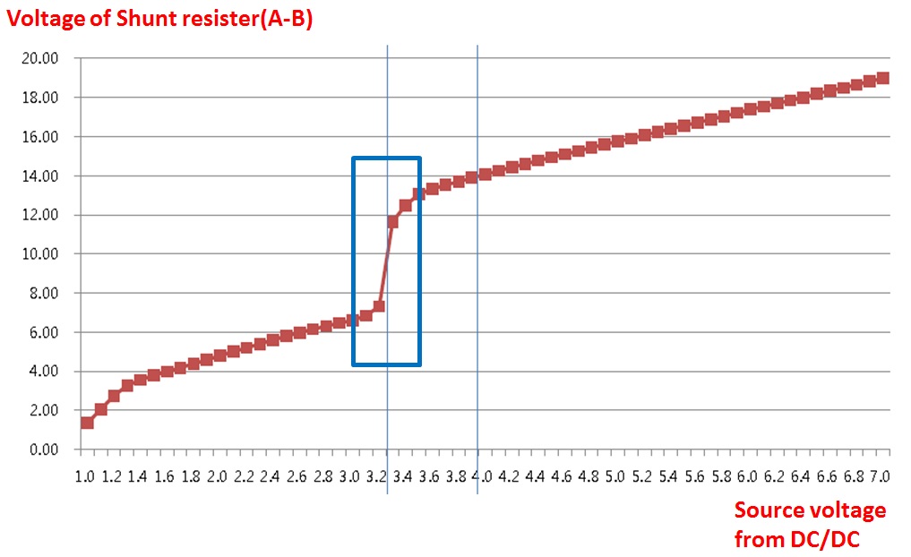
Please review below block and abnormal non-linearity section(Blue box) and let me know your opinion why this section appear.

< phenomenon>
- If INA209 is disconnected, abnormal non-linearity section disappear
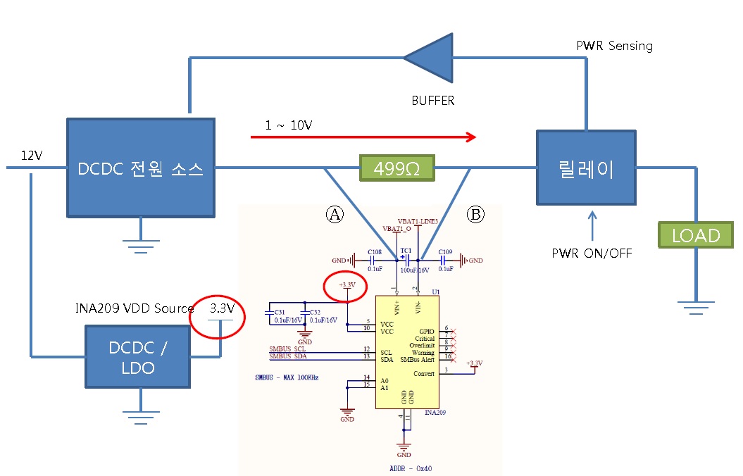
- If Voltage of INA209(3.3V) change to 3.2, abnormal non-linearity section is moved to about3.2V.

If you need more information, please let me know.
Thank you.

< Block>   

<Test result>

  • Hi Nam,

    What are the units of the Vshunt in the graph?

    Regards,
  • Hello Mayrim,

    1. Unit of Vshunt voltage : mV

    2. Unit of source voltage : V

    Thank you.

  • Hi Dino,

    I have a few follow up questions and debugging suggestions:

    1. Does this issue still occur if you remove the feedback path (i.e. break the path from the buffer output to the DC/DC)?
    2. How are you changing the Source voltage from DC/DC? Note that changing the 12V source would change the INA209 supply voltage. Could you share a plot of the INA209 VS vs Source Voltage from DC/DC (Voltage at point A)?
    3. I would also suggest running your test with the INA209 supply pin connected to an independent 3.3V lab supply, if possible. Just to confirm this is not the problem.
    4. In addition, could you also share plots of the INA209 DC input currents (IN+ and IN-) as you sweep the Vcm from 1 V to 10 V?

  • Hi Mayrim,

    Thank you for your reply. I will update result after testing.

    For clarify, this phenomenon is abnormal operation. Is it right?

    Thank you.

  • Hi Nam,

    That's what I am trying to find out with their experiments. If changes in the 12V DC power supply are not affecting the Vs of the INA209 this might be a device characteristic.

    It was brought to my attention that similar behavior is present in other devices such as INA226. It is possible that what they are seeing is the change in input bias currents as the VCM moves through the transition region from supply bias to input bias. Figure 12 of the INA226 (Ib vs Vcm curve) shows this behavior. It is possible that they see a big change because of the low current they are monitoring and the large shunt resistor they have.
  • Hi Mayrim,

    I got answer from customer. Please refer to the below answer and let me know your opinion.  

    1. Does this issue still occur if you remove the feedback path (i.e. break the path from the buffer output to the DC/DC)?
      A) They can't remove the feedback path because of DC/DC regulagtion. but if they remove A path, this issue don't occur.

    2. How are you changing the Source voltage from DC/DC? Note that changing the 12V source would change the INA209 supply voltage. Could you share a plot of the INA209 VS vs Source Voltage from DC/DC (Voltage at point A)?
      A) There is not plot but they checked there is no change of INA209 VS as changing source voltage from DC/DC (voltage at Point A)

    3. I would also suggest running your test with the INA209 supply pin connected to an independent 3.3V lab supply, if possible. Just to confirm this is not the problem.
      A) If circuit of INA209 is isolated from other circuit only connecting A and B point to VIN+/- using wire, we can show constant voltage between A and B even changing source voltage from DC/DC(1 to 10V). Is it normal result?       

    4. In addition, could you also share plots of the INA209 DC input currents (IN+ and IN-) as you sweep the Vcm from 1 V to 10 V?
      A) About 2uA

    Thank you.

  • Hi Dino,

    I noticed that you edited your first response to question #3.  Can you please clarify?  In your previous response you mentioned " If they use an independent 3.3V from lab supply, this issue don't occur. but I don't understand if this issue don't occur as using independent supply, I think the INA209 VS should be changed as changing source voltage from DC/DC (voltage at Point A). Let me know your opinion". If they use an independent 3.3V from lab supply and the issue don't occur this is an indication that the INA209 supply voltage is changing when the DC to DC supply change. 

    We need to understand what is the actual behavior here due to the DC/DC voltage change. It is not possible that there is no change of INA209 VS as changing voltage from DC/DC (response to question #2) but the issue don't happen when connecting an independent supply to the INA209 (response to question #3). 

    Your new question: A) If circuit of INA209 is isolated from other circuit only connecting A and B point to VIN+/- using wire, we can show constant voltage between A and B even changing source voltage from DC/DC(1 to 10V). Is it normal result?     

    Yes. It is normal response because if there is no change in differential voltage you won't see any change in the output. 

    Regards,

  • Hi Mayrim,

    I am sorry for confusing. there is misunderstanding with customer. The test of using independent 3.3V supply is not completed. I will update result.

    <New question>

    1. You mentioned "It is not possible that there is no change of INA209 VS as changing voltage from DC/DC"
        - Although changing voltage from DC/DC(Voltage at point A), i think INA209 VCC(3.3V) might not be changed because of using other LDO(12V in/ 3.3V out). let me know your opinion.

    2. About edited question,
        - If the constant voltage between A and B is normal response, Is it the abnormal response of going up response even excepting jumping step(Blue box)? Which result is normal response? Constant voltage response or going up response as changing voltage from DC/DC(PointA, 1 to 10V)?   

    Thank you.

  • Hi Mayrim,

    We finished test of using independent 3.3V supply but the issue also occur. please review above article and let me know your opinion about reason of abnormal issue.

    Thank you.
  • Hi Dino,

    I will setup some test in the lab tomorrow morning to try to replicate what your customer is seeing. 

    I might need to setup a call with you to discuss and clarifications as the setup is a bit confusing for me at this time. I will update you with my feedback ASAP. 

    Mayrim

  • Hi Mayrim,

    Is there any update on this issue? please let me know your test result.

    Thank you.

  • Dear Dino,

    I have tried recreating the test here in the lab, but have been unable to replicate the results seen here. As I sweep through common mode on my setup, I do not see a rise in differential voltage. I also see no fluctuations in the bias currents. Is there any other information you could provide from the customer setup that might be adding to this?

    Carolus
  • Dear Cauolus,

    Thank you for your support.
     
    1. You mean the constant voltage between V+ and V- of INA209 (differential) is normal operation. A rising voltage in differential voltage excepting  
        jumping period(Blue box at first article) is abnormal operation. Is it right?

    2. What is your measured value in differential voltage?  

    3. The customer said if the circuit of INA209 is isolated from power source, they see a constant voltage(below 1mV) in differential voltage. 
        but if the GND of INA209 circuit is connected GND of other circuit, they see a rise in differential voltage. Need isolation to operate normal?? 
        Let me know your opinion. 
     
    4. Customer setup
        - Please refer to the attached file. remove RS1 and  insert 499 ohm, As I mentioned above if the GND of attched circuit is disconnected
          GND of other circuit(DC/DC, LDO and etc), the differential voltage is costant(below 1mV).
         INA209 Shield V1.0.PDF

    Please let me know your opinion about above question.
    Thank you.

  • Dear Carolus,

    Is there any update on this issue? please let me know your opinion about above qeustions.

    Thank you
  • Dino,

    Did some digging, got some answers. I'll answer your questions first and then give you my thoughts as to your problem:\

    1. Yes and no. While I do also mean the non-linear portion of the graph, I am also talking about the rest of it. The common mode should have no bearing on the differential voltage. While their is the period of nonlinearity highlighted, the graph presented shows a linear increase throughout the totaliy of the graph as they sweep through the common mode. This should not happen. This is more than likely due to their choice of such a large shunt resistor (499 ohms). If the impedance of the load is only a few thousand ohms, then this resistor will absorb a significant portion of the load as the line voltage changes.

    2. As I did not know the customer load value, I used a set of precision voltage supplies to test a range of voltages through the 1 to 10 V range. All values performed to datasheet spec.

    3. No, the INA209 should be referenced to ground.

    4. Again, the part should definitely be grounded.

    As for the issue, here's what I found: in almost all current shunt monitors, there is an internal switching topology that occurs approximately at the point where Vs = Vcm. Up to the point where Vcm < Vs, the part is primarily powered by Vs. At the point where Vcm > Vs, the part switches inside and begins to draw current from the common mode. This is what allows these parts, unlike most op amps, to accept common modes that exceed the supply. For some reason, we did not characterize this on this part, but I have posted a graph of the phenomena from the INA210 to demonstrate the effect:

    Please keep in mind this is from the INA210, so it is NOT the actual behavior that the INA209 will exhibit. I just included it to help you visualize what is happening.

    In addition, this nonlinearity is being exacerbated by the customer's choice of such a large shunt resistor with respect to the load. By their graph, a 1V change in the common mode contributes a 4mV addition to the differential. As I stated in point 1 above, typically the change in of the common mode should have minimal bearing on the differential voltage. By using such a large shunt, they are actively drawing voltage out of the circuit that should be going to the load.

    Ultimately, I would recommend that they push the value of the shunt down to a much smaller size to mitigate the effects of what they are seeing here.

    Hope this helps,

    Carolus

  • Carolus,

    Thank you for your strong support and sorry for confusing. All test is under no load.
    The customer tested 0.05Ω, 0.25Ω, 4.99Ω, 49.9Ω, 499Ω as a shunt. And They get a same trend but the magnitude of non-linear portion decrease as changing shunt value(For example, 10mV at 499 ohm, 1mV at 49.9 ohm). You mean that this result is caracteristic of INA209and similiar parts. Is my understanding right?

    Thank you.
  • Dear Dino,

    Yes. It is due to the fact that at that point of operation, the common mode is now exceeding the supply voltage. Therefore, when this occurs, the part switches internally and, as a result, begins to draw additional current at the inputs of the INA209. This results in an increase of input bias current, and therefore you see a small jump in the differential voltage at that point. As you said, they see the impact of the magnitude shrink as their choice of shunt resistor goes down, so going smaller is usually a good decision to mitigate this.