This thread has been locked.

If you have a related question, please click the "Ask a related question" button in the top right corner. The newly created question will be automatically linked to this question.

LM2903-N: Figure Error in the Datasheet

Part Number: LM2903-N

Dear e2e Team,

In the Figure 4 and 5 of the datasheet the logic presented is:
IN+ bigger thet IN- => Output Q8 open => OUT 5V
IN- bigger thet IN+ => Output Q8 close => OUT 0V

However, In the Figure 13 the logic presentesd is the oposite:
IN- bigger thet IN+ => Output Q8 open => OUT 5V
IN+ bigger thet IN- => Output Q8 close => OUT 0V

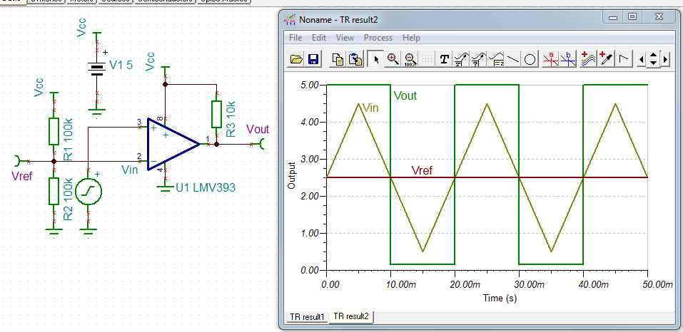
If I refer to the section ; 9.2.1.2 Detailed Design Procedure, we might have the circuit below.

And the simulation with TINA TI gives : 

But if we have a look at the figure Figure 13 it's the opposite.

The  Figure 13 of the datasheet is it correct or there is something I didn't get?

Thank you very much for your help,

  • Hello BMA,

    The graph is correct. What is not shown too well in the the graph is the input "overdrive" voltage. "Overdrive" voltage (+5mV, +20mV or +100mV) is the "extra" voltage above the threshold trip point (0V in the graph).  The more overdrive voltage, the faster the response - which is what the graph is showing.

    The input signal starts at -100mV, but it *stops* at +5mV, or +20mV, or +100mV. So at that point, the negative input is *above* the positive input, which would make the output go low.

    In your simulation, you have the inputs backwards. In the graph, the pulse is going into the negative input, and the reference voltage (GND) is going into the positive input. Reverse the inputs and it will then match the graph :^)

  • Hello.

    Paul,

    The Figures Figure 4 and 5 are correct.

    The problem is in the Figure 13. That one refers to an Typicall Aplication Circuit, presented in Figure 11, where the Vin signal goes to +IN and Vref goes to -IN. As the Simulation circuit.

    Thanks,
    Domingos Gonçalves.
  • Hello Domingos and BMA,

    My apologies..I should have been more clear.

    The Figures 4 and 5 are correct. I may have been blinded-by-familiarity on Fig 13.

    Figure 13 *was* correct, as we corrected it several months ago. So, yes, Figure 13 is incorrect...again.

    I will need to investigate why the incorrect graph has re-appeared and get it fixed.
  • Hello.

    The Figure 13 of the datasheet (document: SNOSBJ6F –OCTOBER 1999–REVISED DECEMBER 2014) is incorrect.

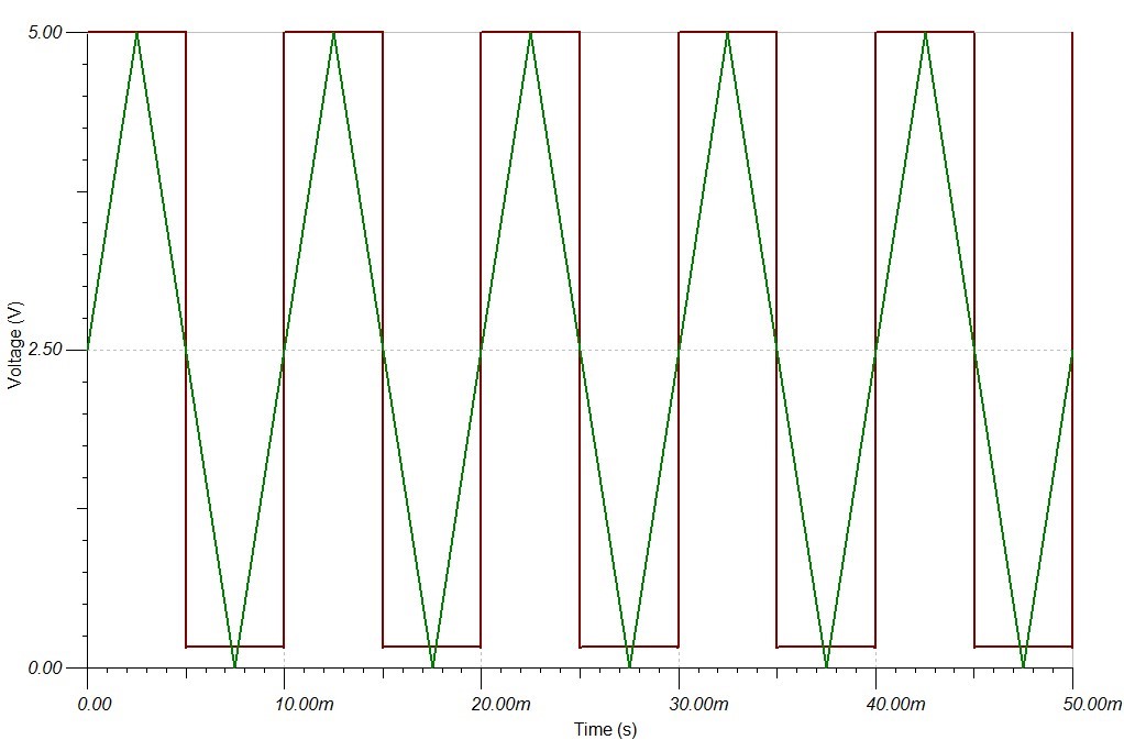
    The correct Comparator Response Figure should be something like this:

    The Correct Output Logic is:

    IN+ bigger that IN- => Output Q8 open => OUT 5V
    IN- bigger that IN+ => Output Q8 close => OUT 0V

    Thanks, Best Regards.

    Domingos Gonçalves.