This thread has been locked.

If you have a related question, please click the "Ask a related question" button in the top right corner. The newly created question will be automatically linked to this question.

LMV602: input offset voltage issue

Part Number: LMV602

hi sir,

our customer meet some LMV602 has one issue for the input offset voltage.

if they set the input offset voltage on the 0.85mv, their circurt gain is incorrect, correct gain is 70, if they adjust input offset voltage to 1.6mV, gain is correct.

and this part input offset is typical voltage is 0.55mv, Max voltage is 5mV, base on the VCC is 2.7V.  their design is 3.3V.

so customer question is why input offset voltage will effect output Gain voltage. another is why close to typical of input voltage value will effect, whether every AMP has minimum input offset voltage value, if customer less this part, it will effect out put Gain data.

why it is appear some IC of LMV602, not all of LMV602 have this issue.

note:because customer can't show details of schematic for LMV602, so I only can tell they set the Gain is 70.

  • Hi Lina,

    is it DC gain? Or AC gain? What is the input signal of this circuit? A DC signal or an AC signal? What is the output voltage? Have you noticed that datasheet mentions that the output cannot go fully down to 0V?

    Is R309 big enough to isolate the output of LMV602 from the capacitive load C30_?

    Kai
  • Hi Lina,

    We're going to need more information to help debug what's happening here. As Kai suggested, can you tell us whether or not this is AC or DC input signal?

    What do you mean "set the input offset voltage"? Typically we think of the input offset voltage as a parameter of the op-amp that cannot be changed by the user.

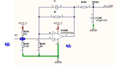
    Looking at the provided schematic, we can determine the value of Rf for a gain of 70, but it is important to know what Cf and R309 are for stability purposes. Also, why is the divider for R304 and R306 set the way it is? By my calculation, on a 3.3V supply, the DC voltage at the input to the op-amp would be very close to ground, which could cause problems. For a single supply application, biasing to mid-supply is usually a better starting point as it allows the largest input voltage range.

    I understand that your customer has concerns about sharing information, but this is a simple non-inverting gain configuration with an isolation resistor, which discuss extensively in our video series TI Precision Labs and we have seen many times. We will be able to provide much better assistance with more information on the circuit.

    Thank you,
    Paul
  • hi Paul,

    correct my above mentioned set the input offset voltage, in fact, it is set the DC bias voltage. 

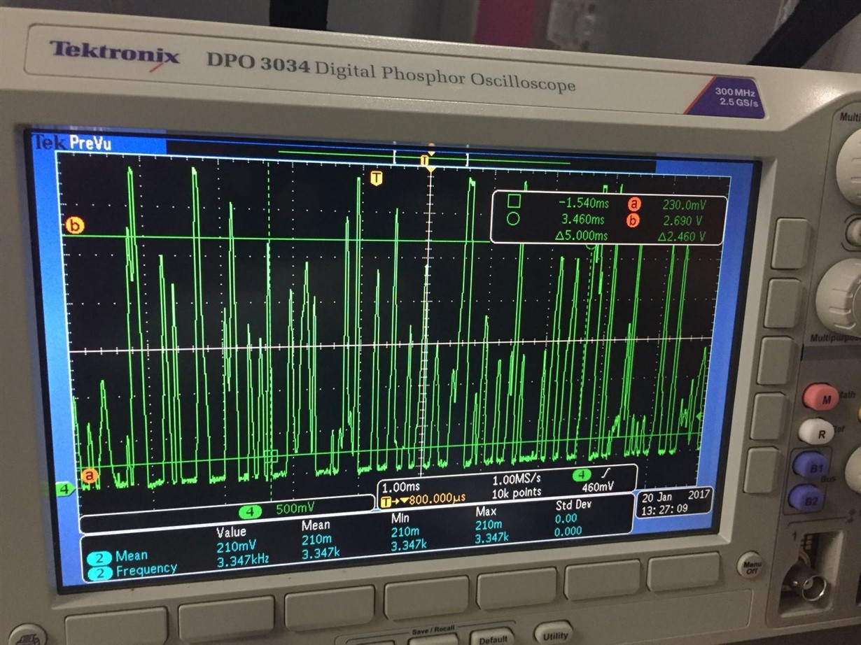
    customer input signal is DC+AC, R305=510ohm is set the DC lever is 0.85mV, AC signal is  ruleless pulse, it is so weak that we can't know details value.(you can refer below output wave)

    BTW, above schematic  R=220kohm, C:220pf, R309=51Kohm.

    now issue is if R305=510ohm, device can't run into enlarged area, if R305 is 1k, it can enlarged normal as below output wave.

    customer want to know, why will cause this issue? how to set the DC bias voltage.

  • Hi Lina,

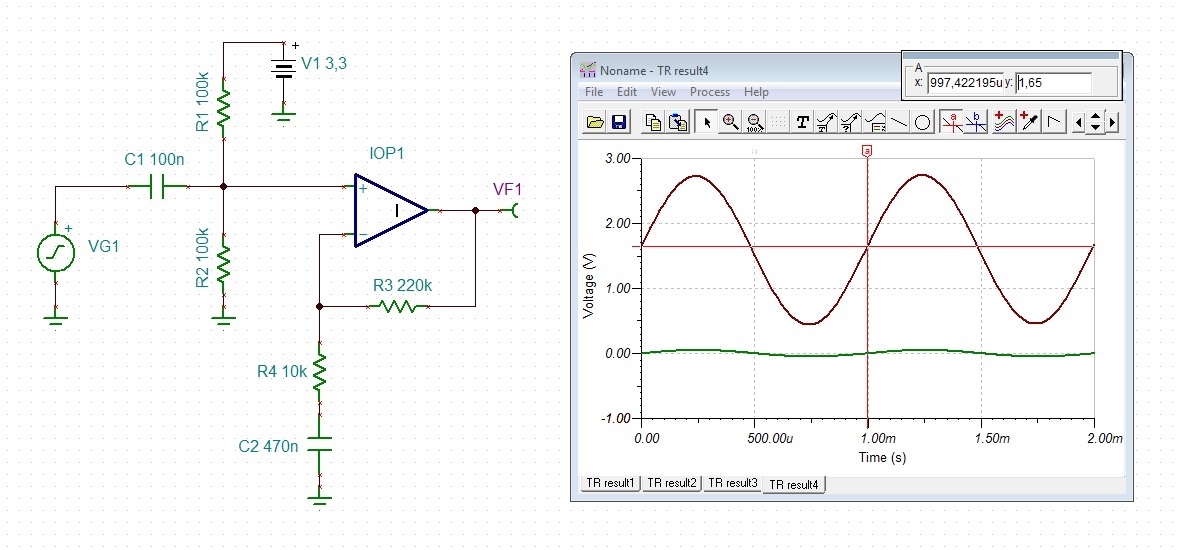
    if your sensor has only AC information and no DC information you should generate a bias voltage which is much higher than your 0.8mV. Next, AC couple your sensor signal to OPAmp input. The gain setting feedback loop should also amplify only the AC information:

    In the circuit above the bias voltage is 1.65V. The amplified sensor signal at the output of OPAmp sits on the same bias voltage. In my example the AC sensor signal has an amplitude of 50mVp.

    Kai

  • Hi Kai:

    I'm the end user of this case. Actually we just have a quick question here.

    We use 0.85mV DC bias voltage because we want the bias voltage as low as possible. Because we want to have more range from 0.85mV ~ 3.3V.
    According to above's input, it seems 0.85mV is not suitable. Is there any minimal value of input DC bias voltage? We could not set to half of VCC in this case.

    As we found that if we set 0.85mV there, not all of the chips are working incorrectly. Most of them are correct. Some of these are working incorrect but after we change the bias voltage to 1.6mV (510 Ohm to 1K Ohm), it works. So that's why we want to know what the minimal value of this chip.

    Thanks.
  • Hi User,

    the OPAmp cannot handle negative voltages at the input. The output is not able to handle negative voltages either. Even output voltages down to 0V are not possible. So, you must generate an input bias voltage which does not violate the common mode input voltage range of OPAmp.

    What is your input signal? Does it have DC information? Or only AC information?

    Kai
  • Hi Kai:

    Thanks for your reply. 

    Actually the signal we want to amplify is a very weak positive pulse from a photo diode. And we only need to get positive signal from OP output.

    We configure the DC bias voltage to 0.85mV because we want the DC reference as lower as possible at output side. Otherwise, it will reduce the signal range. 

    Now the issue is that sometimes, the chip could not amplify this weak pulse correctly if the bias voltage is 0.85mV. But if we set this voltage to 1.6mV, it works. Also we do swap the "problem" chip with "good" one, the result is same. The "problem" chip is not working always.

    That's why we popup this question. We just want to know what's the minimal DC bias voltage according to our case? I need this spec back to my leader to review the design again.

    Email might be not good enough to describe our problem. If you are located in China, could you please provide your contact information? We could discuss a little bit more about this. Thanks.

  • Hi User,

    unfortunately, I'm not living in China. :-)

    If you want to amplifiy the signal of a photo diode, have you thought about using a TIA (transimpedance amplifier)?

    www.ti.com/lit/ug/tidu535/tidu535.pdf

    Kai
  • Hi Kai:

    Thanks. I think we will consider your recommendation. But in this case,I need to get clear feedback from TI what is the minimal DC bias voltage by using LMV602 to get the chip working correctly. I need this data and go back to our design team to fix the issue. Either change chip or update our existed design. It's quick urgent, so please provide the answer as soon as possible. Thanks a lot.
  • Hi User,

    for a supply voltage of 3.3V the common mode input voltage range of LMV602 is 0V...2.3V. The output voltage range is 30mV...3.27V with a load of 10k connected to 3.3V/2=1.65V.

    Kai
  • Hi User, Lina,

    I took another look at your schematic and provided information and realized that I am still not sure what is going on here. First, you've been describing the input signal from the photo diode as "weak" but the oscilloscope picture above shows an input of almost 3Vpk! If you have a 10x probe, then that would mean the signal is 300mVpk. Can you provide the approximate frequency and amplitude of the input signal?

    You've also selected a feedback capacitor C which sets a corner frequency of just 3.3kHz. A rough estimate of the frequency of your input signal from the oscilloscope image makes me believe that the input signal is at least 4kHz and if you're trying to capture the individual pulses and not just peak detect, then you're going to need much more bandwidth to fully capture the signals.

    Finally, on your output, R309 and C308 form a low pass filter with a cutoff frequency of just 3Hz! Why is that set so low? Is there a requirement for such a large load capacitor?

    Help me understand your design goals - are you looking to amplify each individual peak by ~70? Are you just looking to peak detect and hold? My recommendations moving forward would be the following:

    * If you are DC coupled, change your filter frequencies (C and C308) and get rid of the DC biasing altogether. For a non-AC coupled system, there is no need for DC bias.

    * If you are AC-coupled, set the input common mode voltage (IN+ DC bias point) so that you get maximum output swing, which would be roughly mid supply. Remember that the DC bias point will also be amplified by the gain of the op amp, so DC Bias Voltage = (Supply/2)/Gain. In this case, I would recommend setting R304 to 1MEG and R305 to 2.5k as a rough starting point.

    I've attached an AC coupled version of your circuit in a simulation file for you to work with. Let me know if you have any questions.

    LMV602_E2E_AC_Coupled.TSC

    Best,

    Paul

  • Hi User, Lina,

    Do you have any further comments on these questions? If not, I will close this thread and you can post a new question when you're ready.

    Thanks,
    Paul