This thread has been locked.

If you have a related question, please click the "Ask a related question" button in the top right corner. The newly created question will be automatically linked to this question.

INA129: WHY did not i recognize the differences of INA128 vs INA129 and OPA2134 vs TL074?

Part Number: INA129
Other Parts Discussed in Thread: OPA2134, , INA128, TL072, TINA-TI

Hello.

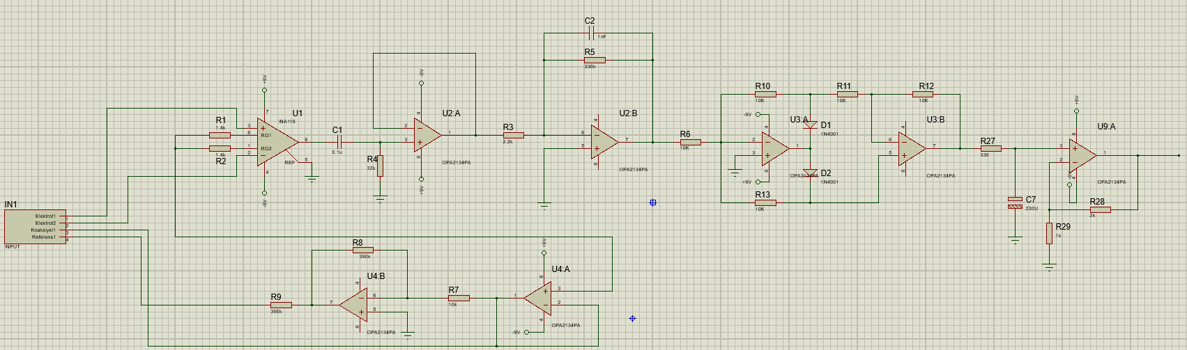
 I use a EMG amplifier circuit. In the circuit i use INA128 as In-Amp and TL072 as Op-Amp. I had  almost 500 mV dc offset output of the circuit. The EMG signals that taken from the surface from the body maximum amplitude is 1mV and my circuit total gain is 3000. I wanted to upgrade these IC and i decided to use INA129 and OPA2134. But the dc offset is not better. Sometimes it was worse. What is the problem? My circuit is attached! 

Thanks in advance!

  • Hi Mehmet,

    why don't you have another high pass filter at U2B? This would extremely decrease the offset problem.

    Why is the gain of U2B so high and the gain of U2A so low? Why do you use an inverting amplifier for U2B?

    Kai
  • I don't really know what the answers of these questions are. I used the circuit in the PDF down below. In the circuit, low pass filter cut off frequency is nearly 500 Hz and high pass filter cut off frequency is nearly 45 Hz. Why should I use another high pass filter? 

    01323147.pdf

  • Hi Mehmet,

    the circuit is not optimized for low offset voltage. The offset voltage of two OPAmps is amplified with a gain of 150 which can result in a huge output offset voltage.

    I have redrawn the circuit to give a much lower output offset voltage. As you can see from the TINA-TI simulation the gain and the frequency response is nearly unchanged:

    Kai

  • That's good news! Thank you so much! But I have 3 question again.

    1) Why do they (in the article) use a buffer between filters? (So you said it is unnecesary).

    2) If I did these modifications would i see the differences INA129 vs INA128 and OPA2134 vs TL072?

    3) Do you think INA129 and OPA2134 are the best options?

  • Hi Mehmet,

    I guess the designer of the circuit was a bit unskilled.

    As I don't know more about the whole apllication I cannot say whether one of the INAs is better, but you will not see the offset voltage of the INA anyway, because it's blocked by C1.

    In my circuit C3 blocks the offset voltage of first OPAmp. So, the offset voltage of this OPAmp is also irrelevant. C3 does not fully block the offset voltage of the second OPAmp, but it makes that the offset voltage appears on the output only amplified by a gain of 1. So, with a TL072 the worst case offset voltage will be 13mV and with the OPA2134 3mV.

    Kai
  • Thank you so much! I appreciate every suggestion you gave.
  • Hey Kai.

    Do you think this circuit is well designed? Its dc offset is under 3mV. But high pass filter is in the end of the circuit. Is it problem? The cascade connection for band pass filter should be respectively high pass-amplifier-low pass filter ( www.electronics-tutorials.ws/filter/filter_7.html ). If i put the high pass filter before the rectifier circuit dc offset is 1.7 V. It is so high.

  • Hi Mehmet,

    please compare your first circuit with the last: In the first circuit there is a low pass filter behind the double wave rectifier. In your last circuit there is a high pass filter. This should also be a low pass filter?

    Kai

  • Hello Kai,

    I only simulate some part of the circuit. The part of the circuit that i simulated here:

    First i changed only 150 gain low pass filter stage. But my offset did not change. Look here:

    Then i put the high pass filter in the end of the simulation part of the circuit. High pass filter is stopped the offset voltage. Look here please:

    But my circuit's stages are like that: Low Pass Filter-Amplifier-Rectifier-High Pass Filter. Is that a problem for my circuit? I know it is recommended that it should be High Pass-Amplifier-Low Pass.

    I need your suggestions! Thanks in advance!

  • Hi Mehmet,

    the first circuit you have presented to us contains two gain stages followed by a full wave rectifier with low pass filter. The purpose of the full wave rectifier with low pass filter is convert the amplitude of the signal into a DC voltage. So, you urgently need this low pass filter and cannot exchange it by a high pass filter. This would not only eliminate the offset voltage but also the wanted signal.

    Kai
  • Hello Kai,

    I red-placed the circuit in TI Sim. I added your suggession that you had gave before. Circuit is here:

    - Amplitude of the EMG signal that is received from body is about 1mV. After INA128 stages its amplitude about 20mV. So my input signal amplitude is 20mV. 

    - Firstly i do not understand why we ve used 47pF in the first amplifier?

    - Secondly at VM4 my signal amplitude is almost 300mV and that is not suprise but at the VM3 point signal amplitude is almost 200mV. Why? It should be 300mVxGain.

    - I redesigned the full wave ractifier from TI, tidu030.pdf document. It is cool right?

    - At the last stage i added my envelope filter. It is 2Hz low pass filter. Thanks to this filter, i can easily use this signal in the microcontroller.

    - In the end i have two question...

    1) Does this circuit do same work compared in the first circuit?

    2) My main goal was to attenuate the offset voltage of the circuit. Will this design work for this goal?

    MY SIMULATION FILE IS ATTACHED. THANKS IN ADVANCE!

    mehmet_emg.TSC

  • Hi Mehmet,

    yes, your circuit looks good. I would R6, R7 and R8 increase to 10k, though. And I would increase R9 to 3k3 and decrease C5 to 22µF.

    To your questions:

    -The 47p cap is a phase lead capacitance which stabilizes the OPAmp.

    -You should not check the gains at high frequencies where C3 already provides a damping. Check the gains at 100Hz, or so.

    -Yes, the circuit should work.

    -Yes, the offset voltage will be much smaller now. For even lower offset voltage you should take the OPA2134. What offset voltage can you accept?

    Kai
  • Thanks for answer Kai,

    C2 value is 2.2uF. How did u calculate this value? Is there any way to calculate that? 

    -My circuit output max value is almost 3V. It would be better if the offset value does not exceed 100mV.

  • Hi Mehmet,

    I didn't want to change the frequency response of the original circuit. So, I made C2 ten times bigger than C1. (C1 and C2 of your last schematic.) But you can modify C2 to your needs, of course.

    Regarding the offset issue: I would take the OPA2134.

    Kai
  • Mehmet

    We haven't heard back from you so we assume this answered your questions. If not post another reply below.

    Thanks
    Dennis