This thread has been locked.

If you have a related question, please click the "Ask a related question" button in the top right corner. The newly created question will be automatically linked to this question.

LM2902KAV: Variation of voltage in Opamp

Part Number: LM2902KAV
Other Parts Discussed in Thread: LM2902

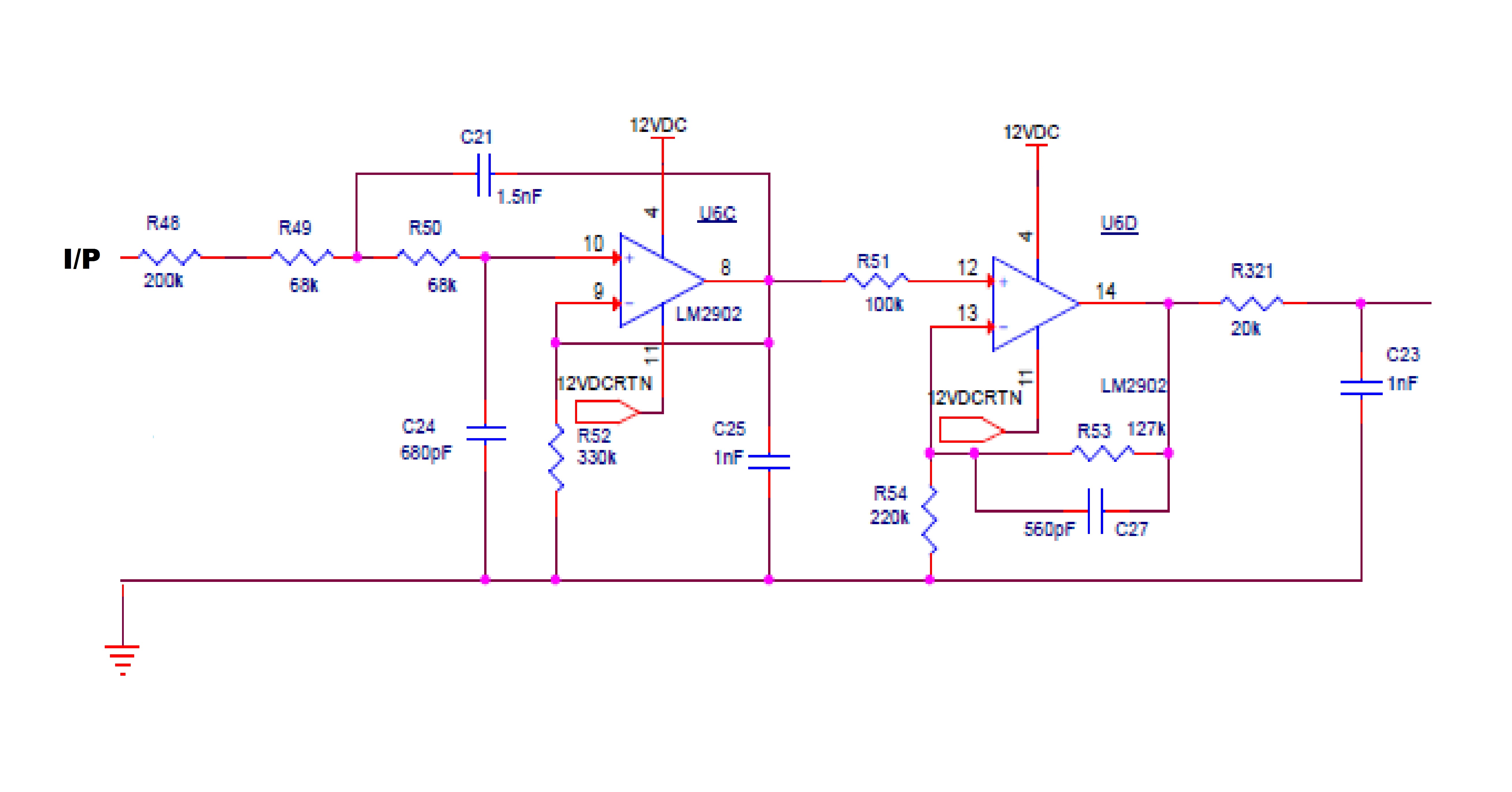
I am using LM2902KAVQDRQ1 for analog voltage amplification as shown in the circuit. The full circuit has a gain of 1.62 and the input range is from 0 - 1.88 V. The problem is that there is a variation of 5-20 mV at the output side(PIN NO 14). The resistor tolerance is 1% and capacitor tolerance is 5% in the circuit.  Can you please suggest any improvements ?  

Regards

Daivik

  • Davik,

    The DC gain of the first stage is 1 with an max 25C offset error of +/-2mV from amplifier offset. Output voltage will increase with input bias current. +V = -IIB * (220k +68k + 68K) = 20nA * 356k = +7.1mV typical increase but value can vary.

    The DC gain of the second stage is 1.577 with an max 25C offset error of +/-3.155mV from amplifier offset
    The the total DC gain is 1.557 and unlikely worst case 1% resistor errors would be +/-2% change in gain.

    If resistors were perfect, then output error (compared to VOUT = VIN * 1.557) would be +/-5.15mV - 1.557 * IIB * 356k
    To get +20mV would require IIB being at least -27nA with high offset voltage or -36nA with perfect op amp offset voltage,all are under the maximum limit.

    To cancel IIB would require adding 357k resistor between pins 8 and 9. For stability reasons add a capacitor in parallel with the new resistor. 560pF (value already in circuit) would work. R52 is not needed as it doesn't do anything useful.

    Please provide a table with input voltage and output voltage to show the variation you have seen. Offset errors come from op amp parameters and gain error comes from resistor matching. This is why a data table is helpful.

    How did you calculate 1.62 as the gain?
    Is '12VDCRTN' node at ground potential or some other voltage?

  • Hi Daivik,

    I noticed C25. It's not wise to connect a 1nF capacitance from the output of OPAmp to GND. Isolate this capacitance from the output of U6C by the help of a resistance, as you did with R321 and C23.

    Kai
  • Kai,

    Thank you, I missed that. I agree that C25 is misplaced (directly on output pin) and harmful (stability concern).
  • Hello Ron,

                   There was typo error,the practical gain of  opamp = 1.02 * 1.57 = 1.6014, I rounded it of to 1.602. The circuit needs to be changed as shown in the image which is attached.I have also attached the data table.  Should tolerance of the capacitors be changed to 1% ?Opamp values.xls

  • 0272.Opamp values.xls

    Daivik,

    I added more data to the excel spreadsheet. First I made a chart of Vout vs Vin then I added a linear trend line with equation shown on chart. This is an easy way to separate gain from offset. Gain accuracy is good .1%, Offset is high 15mV

    I misadded to get R331 value before. 200k +68K =68K is 336k , so closet 1% resistor is 332k or 340k  

    R51 can be improved to be 220k||127k which closest 1% is 80.6k

    Also remove shorts to ground on C186

    All these changes reduce offset voltage. Lower value resistors will also improve offset. The capacitor accuracy won't affect DC gain or offset.  

    We can now talk about the AC component of the input signal. I see you want to pass low frequencies and block high frequency input signals. My only concern is that output crossover might be an distortion issue.

  • Hello Ron,

                    R51 cannot be changed to 80.6k as there is a requirement from customer to have a load impedance of 100k between 2 circuits. I will change R331 to 340K and connect C186 in parallel to R331 without connecting to ground. The capacitor value of C186 should be 560pF or 1nF ?

    Can you  elaborate on the output crossover distortion ? The inputs given are DC voltages.

    Regards 

    Daivik

  • Hi Daivik,

    R51 is no load resistance. Quite honestly, apart from helping to cancel the input bias currents of U6D, it makes no sense at all. R51 should equal the parallel resistance of R53 and R54. So, it should not harm to reduce R51 to 80.6k, as recommended by Ron.

    Kai

  • Daivik,

    If input is DC then all will be well. My concern was about input rising fast enough that the current through C21 would exceed the current of the "50uA current regulator" temporarily [see device schematic on page 10 of the data sheet]. This would cause the output of U6C to spike up as it takes a few microseconds for the LM2902 to switch between current sink (PNP) and current source (NPNs). The typical value per data sheet is 30uA and the series resistance between input and cap is 268k. So it would (typically) take 30uA * 268k = 8V input quick rise to overpower a 30uA sink. Because you stated that your input range is less than 2V, then should not be any crossover, even if input rise 0V to 2V instantaneously.

    The only purpose of C186 is to prevent any phase lag between output of U6C and the inverting input (a couple picofarad) at the bandwidth of the LM2902(typically 1.2MHz). Just about any cap value will do that.

  • Hello,

            I have made changes that have been recommended and the full circuit is in the attachment. I understood the crossover distortion, is there any application note for it?


    Regards

    Daivik

  • Hi Daivik,

    as Ron has already mentioned, there are some shorts in your schematic that must be removed:

    Kai

  • Hello Kai,

                   I will remove these shorts to ground. Thanks for the input.

    Regards

    Daivik