This thread has been locked.

If you have a related question, please click the "Ask a related question" button in the top right corner. The newly created question will be automatically linked to this question.

VCA2615: Maximum input voltage and input capacitance

Part Number: VCA2615

Hi,

I have two questions regarding VCA2615.

1 Maximum input voltage

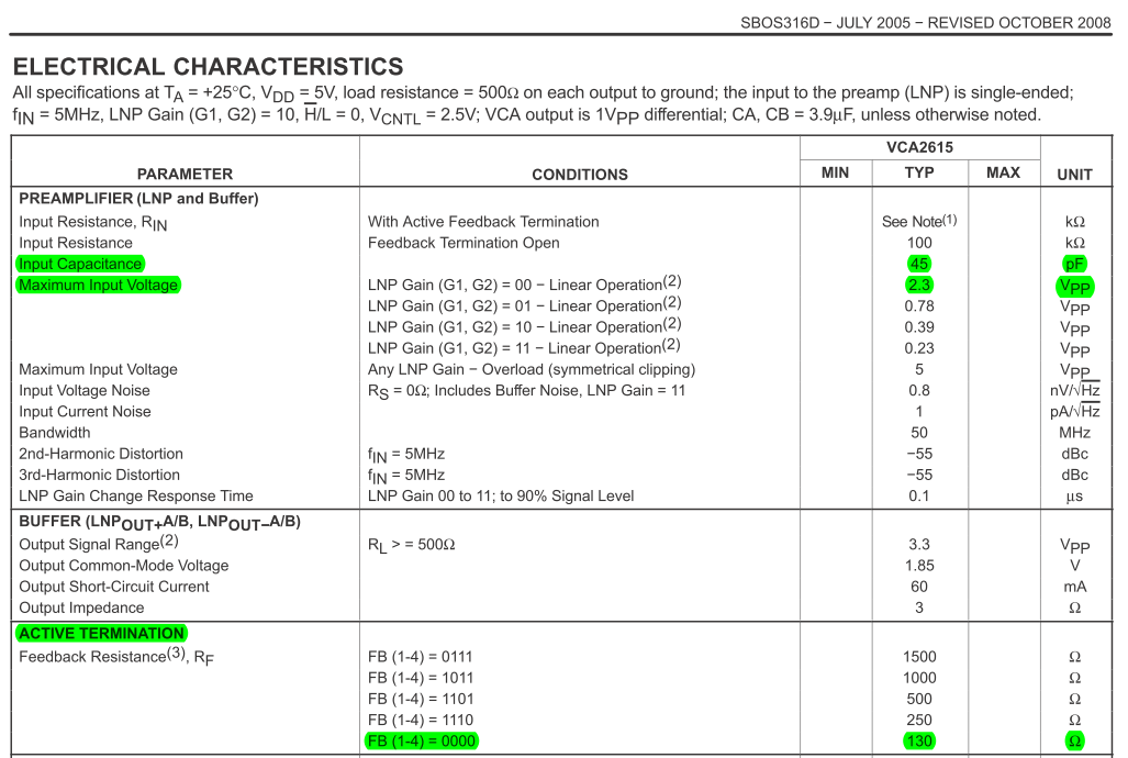
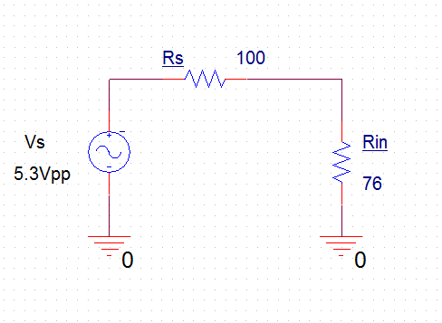
Data sheet SBOS316D page 3, VCA2615 LNP Gain (G1, G2) = 00, maximum input voltage is 2.3 Vpp.

If there is a source signal Vs with a 100 Ohm series resistance Rs, VCA2615 active termination is RF 130 Ohm FB(1-4) = 0000, ALNP = 1.41 V/V (3 dB), RIN = 76 Ohm (formula (5) at page 18), voltage partition between source and termination resistance permits to have a source signal of about (2.3/76)*176 = 5.3 Vpp.

Is my interpretation correct?


2 Input capacitance

Data sheet SBOS316D page 3, Input Capacitance typical value is 45 pF.

The source signal series resistance with VCA2615 input capacitance realize a low-pass filter. Which is the maximum input capacitance value in order to evaluate the lower low-pass filter band?


Thank you in advance,

Daniele.


  • Hi Daniele,
    How are you?
    Thank you for using VCA2615 device.
    For your question #1:
    Yes, following the data sheet at page 18
    and also according to your settings (FB[1-4]=0000, gain=3dB, Rf=130ohm)
    Rin is around = 76 ohm.
    For your question #2:
    If the input capacitance only comes from the VCA2615's input pin (which obtains typical 45pF)
    and also input resistance has only 50ohm in series,
    then its low-pass filter could be around ~70MHz range.
    Of course, if the input resistance becomes 100ohm,
    then its low-pass filter could be around ~35MHz.
    And on the VCA2615 data sheet,
    it mentions LNP bandwidth is typ ~50MHz.

    Thank you very much!
    Best regards,
    Chen
  • Dear Chen,
    thank you for responses.
    Could you please provide me further explanations ?

    1. Maximum input voltage
    If I use a 100 Ohm series resistor RS and I set RF 130 Ohm (to have RIN 76 Ohm), input signal Vs can be 5.3 VPP?
    Modifying VCA2615 example project on TINA simulator I don’t see source signal Vs partition.

    In my application maximum input signal is 5 Vpp, it has 100 Ohm series resistance, it is AC coupled and I prefer avoid external attenuator but interface directly to VCA2615.

    2. Input capacitance
    I would kwon the maximum input capacitance value, instead of typical, in order to evaluate if the worst case minimum resulting bandwidth is sufficient for my application.
    For instance if Cmax is 90 pF I’ll have half bandwidth respect to 45 pF typical value.

    Thank you very much,
    Daniele.
  • Hi Daniele,
    How are you?
    Could you please send us more detail information (such plots)
    for your question #1?
    because we don't know where the issue comes from.

    Thank you!
    Best regards,
    Chen
  • Hi Chen,

    here after screenshot of TINA circuit modified from TI VCA2615 example (100 Ohm series resistance).

    Changing FB1..FB4 from 0 to 5 V (RF from 130  Ohm 100 KOhm), doing transient analysis VINP signal amplitude doesn’t change.

    Thanks,

    Daniele.

  • Hi Daniele,

    How are you?

    Yes, we were following all the same test conditions as you mentioned as many as we can.

    (Please look at the following plot).

    such as G1,G2=00

    FB1..FB4=0000

    RF set to be=130ohm

    (so Rin=76ohm still as you had already).

    But our input signal Vs is = 2.1Vpp at 3MHz

    and Rs is = 50ohm

    Therefore when we measured the VM1 point,

    we got 1.38Vpp (also at 3MHz)

    which is very close to the ideal result.

    So if you can test VCA2614EVM board in your side,

    please use your EVM and set it to the settings as you need to verify

    with your VCA2615 simulation.

    Thank you!

    Have a nice day!

    Best regards,

    Chen