This thread has been locked.

If you have a related question, please click the "Ask a related question" button in the top right corner. The newly created question will be automatically linked to this question.

OPA842: Non-inverting resistor calculation

Part Number: OPA842
Other Parts Discussed in Thread: OPA615,

Hi,

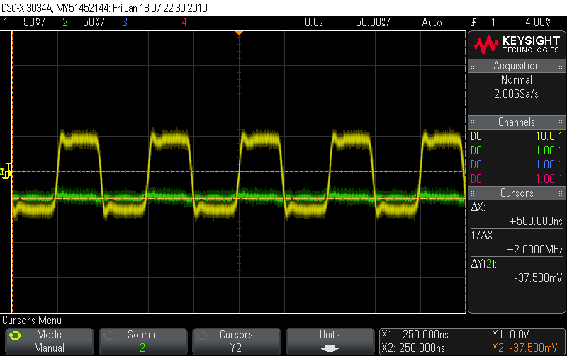
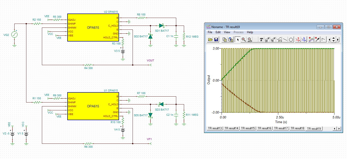
I'm trying to build a peak detector used for square wave @10MHz and the amplitude as low as 100mVpp. I followed the circuit in the OPA615 datasheet but run into the following issues:

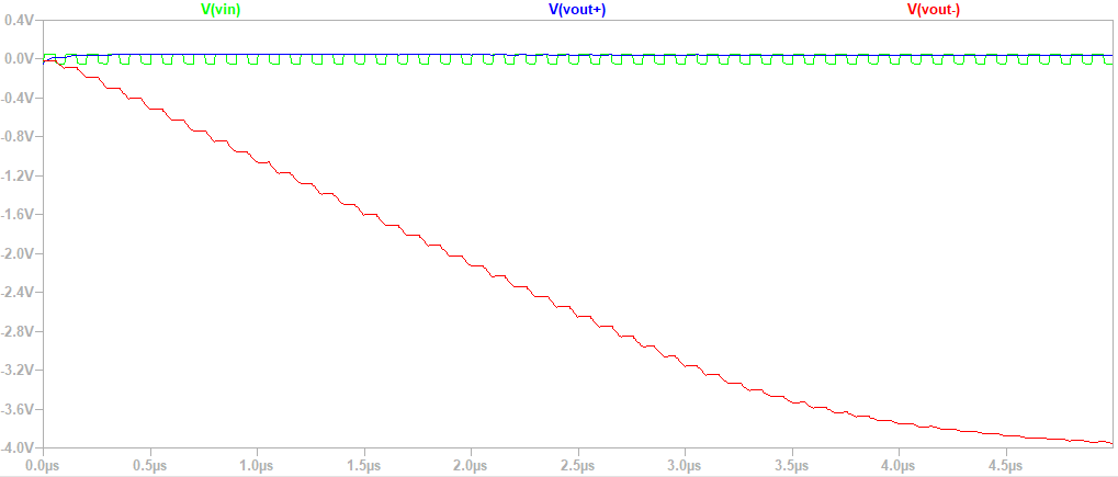
1. The positive peak detector has a drop of ~5 to 10mV depending on the diodes being used. So far, I found that the diode JDH2S02SL gives the least drop.

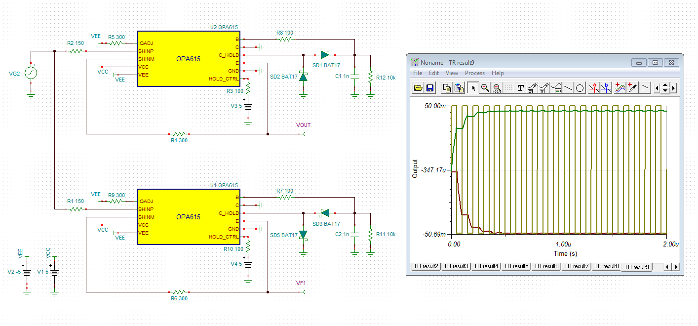
2. Negative peak detector circuit is not working. I've tried both simulation and LAB. This leads to issue #3

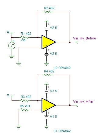
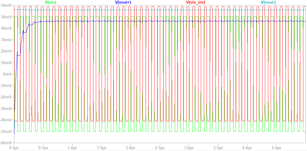
3. So in order to detect the negative peak, I'm trying to use the OPA842 to flip the input signal (G = -1). However, I can't seem to calculate the resistor connected to the non-inverting OPA842 input. The circuit i use is also from OPA842 datasheet (datasheet circuit has a gain of -2 instead). They do mention briefly about that resistor calculation but i can't figure out how.

So my questions are:

1. Do you have any suggestions to achieve a better peak result?

2. How to calculate the resistor connected to non-inverting OPA842 when configured as G = -1?

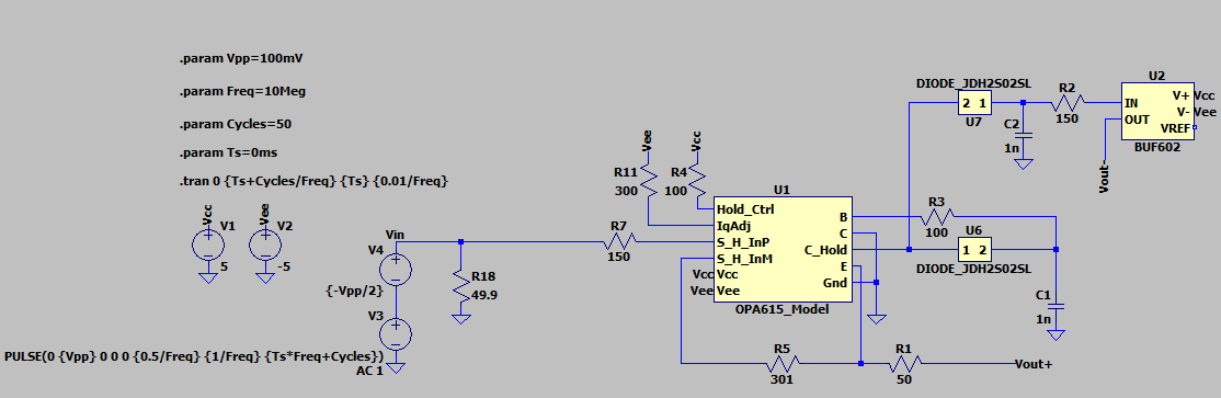
Here's my simulation from LTspice: 

PSpice models used:

OPA615_Model.LIB

OPA842_Model.txt
*-----------------------------------------------------------------------
* OPA842 Wideband,  Low Noise Voltage Feedback Op Amp
* Created 5/1/03    RS
* 
* 
* NOTES:
*   1- Uses a multiple pole-zero topology
*   2- For better convergence during transient analysis set:
*        .OPTIONS  ITL4=40
*   3- This macromodel predicts room temperature performance
*      (T = 27 deg C) for: DC, small-signal AC, noise, and
*      transient simulations
*   4- This macromodel does not predict: distortion
*      (harmonic, intermod, diff. gain & phase, ...),
*      temperature effects, board parasitics, differences
*      between package styles, and process changes
*
* |---------------------------------------------------------------|
* |  This macro model is being supplied as an aid to              |
* |  circuit designs.  While it reflects reasonably close         |
* |  similarity to the actual device in terms of performance,     |
* |  it is not suggested as a replacement for breadboarding.      |
* |  Simulation should be used as a forerunner or a supplement    |
* |  to traditional lab testing.                                  |
* |                                                               |
* |  Neither this library nor any part may be copied without      |
* |  the express written consent of Texas Instruments Corporation.|
* |---------------------------------------------------------------|
*
* CONNECTIONS:
*              Non-Inverting Input         
*              | Inverting Input
*              | |  Positive Power Supply    
*              | |  |  Negative Power Supply
*              | |  |  |  Output
*              | |  |  |  |  
*              | |  |  |  |  
.SUBCKT OPA842 + -  V+ V- Out
 
V_V1         V+ 10 DC 1.4  
E_E3         21 22 POLY(2) 0 18  V+ V- -785m 1 0.5
E_E4         24 25 POLY(2) 18 0  V+ V- -785M 1 0.5
D_D1         16 15 DX 1
D_D3         18 20 DX 1
D_D5         23 24 DX 1
D_D7         0 27 DN1 .5
I_I3         27 26 DC 100uA  
I_I4         29 28 DC 100uA  
D_D2         19 18 DX 1
R_R16         21 V+  45  
R_R17         V- 25  45  
R_R18         23 Out  5  
D_D8         28 0 DN1 .5
D_D9         0 29 DN1 .5
D_D6         26 0 DN1 .5
R_R14         17 0  1000K  
G_G3         0 17 POLY(1) 12 11 0 50M 0 0
G_G4         0 18 POLY(1) 17 0 0 1M 0 0
R_R15         18 0  1K  
R_R12         15 13  75  
R_R13         15 14  75  
R_R10         11 10  750  
R_R11         12 10  750  
I_I1         15 V- DC 3.1mA  
D_D4         22 23 DX 1
E_E1         19 0 POLY(1) V- V+ .5 0.5 0 0
E_E2         20 0 POLY(1) V+ V- -1.0 0.5 0 0
V_V2         16 V- DC 1.5  
G_G2         2 0 POLY(2) 28 0 29 0 0 .001m .001m
G_G1         + 0 POLY(2) 26 0 27 0 0 .001m .001m
Q_Q1         11 + 13 QN 12
Q_Q2         12 2 14 QN 11.867
I_I2         V+ V- DC 15.7mA  
C_C2         17 0  200p  
L_L5         2 -  2.46nH  
C_C13         0 2  1p  

*
.MODEL DX D(IS=1.0000E-15) 
.MODEL DN1 D(IS=2F AF=1 KF=10.5E-17)
* QN NPN model
.MODEL QN NPN
+ IS=7.6E-18
+ VAF=78.71
+ VAR=1.452
+ BF=157
+ RB=1.20E+02
+ KF=9.5E-15
+ AF= 1.0

.ENDS    OPA842

JDH2S02SL_PSpice_20170209.lib

1SS427.lib

  • Hi Duc,

    there seems to be a mistake with R8, R15 and R14. The parallel resistance of these three resistors is 23.5R. But it should be 50R for a 50R line.

    What is your source resistance (of V3 and V4)? Is the input line a 50R line at all? How far is the source away from the OPA615 circuit? Do you have a 50R cable at the input?

    Kai
  • Hi Kai,

    Maybe a little bit of my project background may help. So ultimately, i want to build a peak detector (PKD) to detect the pk-pk output of a TIA (installed on an eval board). The TIA has 50R output impedance and terminated by a 50R (on the eval board). This will become the Vin source to my PKD circuit above.

    1. What is your source resistance (of V3 and V4)?
    => The TIA chip has a 50R output impedance and terminated by a 50R on the eval board. Maybe I should remove R8 and R15?

    2. Is the input line a 50R line at all?
    => See 1)

    3. How far is the source away from the OPA615 circuit?
    => I can bring my PKD board as close to the eval board output as a few centimeters (10cm?). But there's a trace between the eval output to the TIA about another 10cm.

    4. Do you have a 50R cable at the input?
    => The signal source is coming from a test point (after the termination resistor on the eval board) so i'll have to cut one end of a coax cable to solder down to this test point. The other end will be plugged into my PKD board via SMA connector. So if i decide to keep the whole cable length then it may still be 50R? i'm not sure.
  • Hello Duc,

    The resistances used in your schematic do configure the OPA842 in an inverting configuration. The error seen in V_inv is mainly caused by the bias current of the device. With a typical bias current of 35uA, resistances of 402Ohms and an input offset voltage of 1.5mV, you can get an error of up to 15.57mV. I would recommend implementing bias current cancellation on your device. You can see the difference below:

    Best,

    Hasan Babiker

    Duc.TSC

  • Hi Duc,

    assume your TIA has a series termination resistance of 50R (50R source resistance), then this output should be connected to the input of a 50R cable. Connect the output of this cable to the input of your circuit and let R8 be the only 50R cable termination resistance at the output of cable. Remove R15 and move U5 (with R14) close to R8.

    The input bias current cancelling resistance from the +input of U5 to GND should then be 207R.

    Kai

  • Hi Hasan and Kai,

    Thanks for the comments. Adding ~200R resistor did cancel the bias current. From trial and error, I've found that using ~220R gives the closest pk-pk to the Vin. My question is how did you calculate that resistor?

    Thanks,
    Duc
  • Hey Duc,

    The 201 value is the parallel combination of R13 and R14. In Kai's case, I believe he is including R8 and the source impedance into the calculation to provide a more accurate value for your design. So, 402||(402+(50||50)) = 207. You can follow the links below for further info on the topic:

    training.ti.com/ti-precision-labs-op-amps-vos-and-ib
    e2e.ti.com/.../input-bias-current-cancelation-resistors-do-you-really-need-them
    e2e.ti.com/.../internal-input-bias-current-cancellation

    Best,
    Hasan Babiker
  • Exactly, Hasan, thank you!

    Kai
  • Thanks Kai and Hasan for the calculation detail. This now resolved my question #2.

    Back to question #1. When I use the schematic in the OPA615 for pulse detector, the negative detector is not working. Both lab and simulation show similar result. Do you have any idea why and how to fix it?

    Here's the result from simulation:

    Thanks,

    Duc

  • Hi Duc,

    I would do it this way:

    The deviation of output signals from correct values (50mV, -50mV) is simple offset voltage, which can be corrected for in a following DC circuit. This sort of offset voltage is usual for such HF circuits.

    3443.duc.TSC

    Kai

  • Thanks Kai! woke up and saw your simulation result made me a happy man. I can't wait to get to the lab to verify this on the bench :)
    By the way you mentioned that the offset "can be corrected in a following DC circuit", what circuit is that? Did you forget to attach something?

    Thanks,
    Duc
  • Hi Kai,

    Just got back from the LAB. The result is not as good as the simulation's but still good to me. Hopefully once i put them all in a PCB, it would give better performance.

    The only 2 things I wish to know for this issue to close are:

    1) Do you have any info (documents, links, articles...) regarding the "offset voltage correction" circuit you mentioned above for the positive peak?

    2) What is your thought process to come up with the 10K R11 and R12? (like why you put them there and why 10k?)

    Thanks,

    Duc

  • Hi Duc,

    the 10k resistors shall decrease the influence of input bias currents. The best value differs from chip to chip and depends largely on the signal amplitude. Play a bit with the values.

    The best cure against offset voltages is to choose a high signal level! The following simulation shows that the OPA615 can handle input signal amplitudes of more than 3.0V:

    So, you should drastically increase your signal amplitude before going into the OPA615!!

    Take care, these ultra fast chips are optimized for ultra high speed, not for high precision. So, you have to live with a certain unlinearity and offset. It might need some time and efforts to find the optimum operating point and the optimum components values. Good luck! :-)

    Kai

  • Thanks Kai and Hasan for your valuable inputs. You're awesome! I really really appreciate your help :)

    Best Regards,
    Duc