This thread has been locked.

If you have a related question, please click the "Ask a related question" button in the top right corner. The newly created question will be automatically linked to this question.

OPA735: The voltage ripple of the REF5025 and OPA735 for ADS1282

Part Number: OPA735
Other Parts Discussed in Thread: REF5025, ADS1282, LM27762, ADS1261EVM, ADS1278, ADS1281, REF5050, OPA725, OPA837, TIDA-01055, OPA625

Hello sir,

Thanks for your answer before. But now, I meeting a new problem in my design. Please have a look.

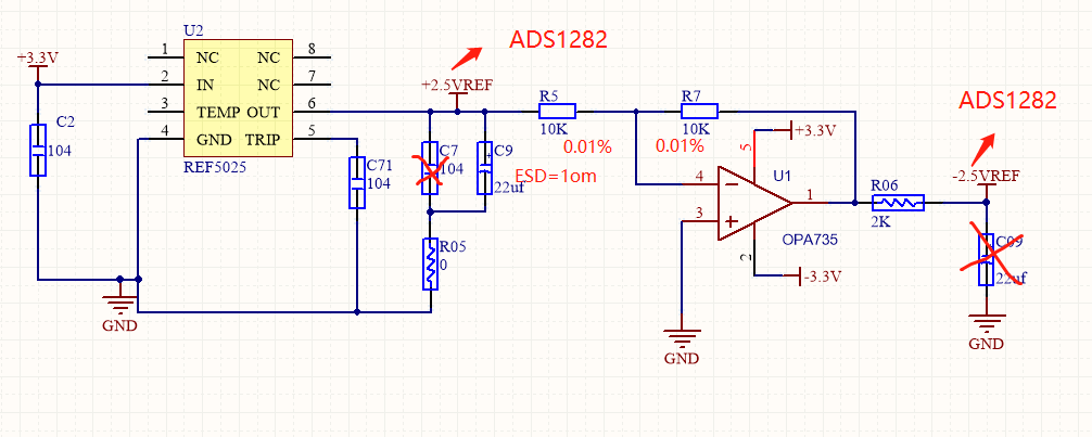
follow circuit refer to Page 18 on datasheet of REF5025; http://www.ti.com.cn/cn/lit/ds/symlink/ref5025.pdf

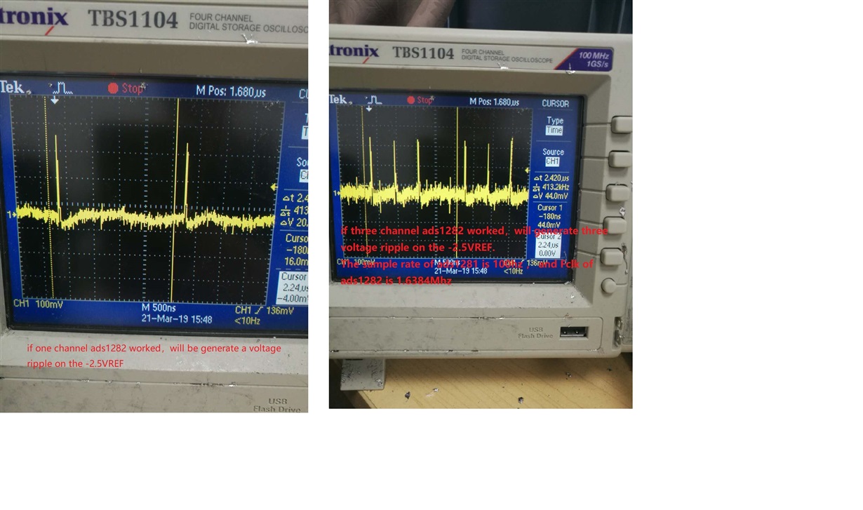
If the ads1282 don't work, the voltage of +2.5VREF and -2.5VREF is very stable and high precise,but when the ads1282 begin to work ,the ripple of  +2.5VREF and -2.5VREF too bad. so do you have any suggestion about this or any other scheme about get high precise negative voltage reference.

thank you very much!

Best regards!

Kevin

  • Hi Kevin,

    Are you using the REF5025 and the OPA735 to power the AVDD and AVSS supplies of the ADS1282?

    You might be able to use to this circuit as a supply voltage, but I'd be concerned that the REF5025 may not be able to supply enough current to the ADC, as it really is only able capable of sourcing about 10mA of current. I would recommend looking into using the LM27762 to generate the +/-2.5V supplies. I've used this circuit on the ADS1261EVM for just this purpose:

    In your current configuration, the 2kOhm resistor on the AVSS supply might be causing problems. I know it may be necessary to stabilize the opamp for any capacitive loads on AVSS; however, this resistance may be too much for the AVSS supply.

  • I think he is talking about the +/-Vref lines, where perhaps the sampling event there is producing glitches due to that 2kOhm series output R. Actually quite a lot of good work has gone on with driving Vref lines with big caps at the pin. Some of those circuits are a bit extreme, but the basic idea is to have the Vref pins see a very low AC and DC source impedance.

    As part of a more general discussion of VFA stability on the high speed side, I included one of the best reference buffer discussions as a reference and example phase margin control - in here -

    www.planetanalog.com/author.asp
  • Hi Kevin,

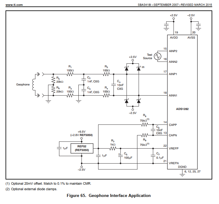
    why not exactly powering and referencing the ADS1282 as shown in figure 65 of datasheet of ADS1282?

    Kai

  • Hello all,

    I might note this 2007 release has not been updated for suggested circuits. Pretty much all of the recent deltasigma (ADS1278) and SAR releases put a lot more effort into the Ref line driving - I suspect there was a slow realization that the sampling and settling aspects on the Vref pins is just as important as the inputs. Might not be true for this part, but I would say it has been one of the main improvements over the last 5years.
  • hello chris,

     thanks for your reply.

     Frist, the +2.5VREF and -2.5VREF just for the reference voltage of ads1281,i used another chip to get + 2.5V and -2.5V  for AVDD and AVSS.

     Second,i had replaced the R06 with 0Ω,but the problem still exist. 

    I can't find the current information about reference on datasheet of ads1281/1282,i think the current is very low......

    thanks again.

    Best regards

  • Hello Kai,
    thanks for your reply,i think this figure is just for example ,you can see, The VREFN connect to the AVSS, maybe this will generate another problem for high resolution data acquisition system. just my opinion, didn't test.
    best regards!
    kevin
  • Hi Kevin,

    The ADS1282 reference inputs present a dynamic load, as the capacitive load switches at the modulator frequency when the ADC perform conversions (please refer to p. 17 of the ADS1282 datasheet). Therefore, the ADS1282 reference inputs need to be driven with a low impedance source. Also, the ADS1282 datasheet recommends using a bypass capacitor across the REF+ and REF- inputs in close proximity to the ADS1282 reference inputs.

    I agree both with Michael and Kai, in the current schematic, the ADS1282 VREFN reference input sees a high impedance of 2kOhm and this impedance is causing the spikes as the sampling of the reference occurs. I believe it will be better to use the REF5050 circuit recommended on figure 65 of the ADS1282 datasheet with the filter and bypass capacitors across the REF+ and REF- terminals. The REF5050 should keep a stable 5V voltage across VREFP/VREFN input pins. Please let us know if the issue persists after replacing the circuit.

    Thank you,

    Best Regards,

    Luis
  • Hello Luis

    Thanks for your reply.

    I agree with you about the voltage ripple is caused by the ADC perform conversion. thanks for your explanation for this.

    I had replaced the R06 with 0Ω,but the problem still exist. 

      if i used the REF5025+OPA735 to get +2.5V and -2.5V , the voltage very stablely and high precision,2.5000xxV and -2.4999xxV. I am not sure the figure  65 on page41 of http://www.ti.com/lit/ds/symlink/ads1282.pdf will get same effective .The  VREFN connect to the AVSS, but the -2.5V of the AVSS maybe this will generate another problem(noise or ...) for high resolution data acquisition system. just my opinion, didn't test.

    In my design,I used differential voltage input. 

    if your have another reference circuit ,please send my emai:peacewyz@163.com

    Best regards!

    Kevin

  • another question:when ADS1281 choose differential input, the +VREF and -VREF must have precision +2.5 and -2.5 or just need make sure the voltage difference is 5V between +VREF and -VREF ?
  • Hi Kevin,

    decreasing R06 to 0R will not help because the OPAmp cannot deliver the dynamic current spikes. That's why the cap C09 is needed. Only this cap can deliver these dynamic current spikes. And R06 is necessary to isolate C09 from the OPAmp because otherwise the OPAmp becomes unstable.

    I think that only the difference between +Vref and -Vref is important. So, it should be able to connect -Vref to AVSS.

    Kai
  • So Kevin, in your current circuit with the OPA725 inverting gain of -1 to generate the -2.5V, that op amp output with no series R and no cap at the VREFN pin will see a sampling glitch due to the closed loop output impedance of the op amp that looks inductive. The 1st step folks try is to add a big cap there but then you run into stability problems for the op amp.

    The next step is to d a dual loop cap load driver to get both the DC precision and a cap as the final load with stability.

    For the most precise reference buffer designs, the next step is then an overall dual loop with a slow chopper op amp as the front end and overall DC loop op amp, and wideband output stage like the OPA837. I worked a little with the TI Industrial designs team on this example. It might be extreme for what you are trying to do, but at minimum you need a cap at both the VREFP and VREFN pins - and I think they buffer the references like the REF5025 also since they also have a rising output impedance over frequency. This TIDA-01055 shows a lot of detail comparing the OPA625 to the OPA837 as the last stage in this more sophisticated Ref. buffer approach - essentially the OPA837 does as well at lower power.

    www.ti.com/.../TIDA-01055

    And again, a lot of the tradeoff work here is getting a low wideband impedance looking back into your reference line that will settle quickly to the Vref sampling event - that then gets back into the phase margin of the active circuits trying to drive a large cap load where I used the output stage in this reference design as an example for analysis in this recent VFA stability article -

    www.planetanalog.com/author.asp

    It would seem the suggested circuits in the ADS1282 could use some updating?
  • Hi Michael,

    as Kevin seems to be a newbie I would recommend him to exactly build what the datasheet is suggesting, even if it might not be the perfect solution. But it might be the best he can achieve with his skills...

    Kai
  • Hi Kevin,

    The ADC uses the difference between VREFP and VREFN to perform conversions, and this voltage difference needs to be stable. In the recommended circuit, the REF5050 keeps the VREFP and VREFN difference stable. Also, The REF+ and REF- require a bypass capacitor across them to provide a charge bucket to provide instantaneous charge to the switch sampling capacitive load. This reference bypass capacitor needs to be in close proximity to the reference input pins. In the circuit suggested of the ADS1282 datasheet, the REF5050 broadband noise is filtered with R7 and C5. In addition the parallel combination of C5 and C7 provide a large charge bucket for the dynamic current spikes.

    If you were to drive the reference pins with an amplifier, you will need to use an OP-AMP that is stable driving the bypass capacitor; and most op-amps will not be able to drive the large bypass capacitive load without the proper compensation. As Kai has mentioned, since there are transient/dynamic current spikes, you can not use a large resistor in series at the OPA output to compensate the OPA735. If you were to use the OPA735 amplifier to drive the reference inputs, you would need to compensate the amplifier using a dual feedback configuration in order to drive the reference bypass capacitor.

    However, I still believe the simplest circuit to drive the reference is the one shown on the ADS1282 datasheet.

    Thank you and Regards,

    Luis