This thread has been locked.

If you have a related question, please click the "Ask a related question" button in the top right corner. The newly created question will be automatically linked to this question.

THS3001: Any idea why it takes 200nS settling time to 0.2% for an 8V step

Part Number: THS3001
Other Parts Discussed in Thread: THS3491, THS3217, THS3091, LM7372

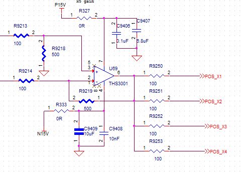
Hi I'm seeing a long slow settling time tail for this part when used as a differential amplifier with  x5 gain 500Ohm feedback and 100 Ohm input resistors. power pins are well decoupled and have less than 10mV of change so it's not a power supply rejection ratio issue. Resistors are metal foil 0.2ppm/C temperature coefficient so super stable. I did consider it being input bias drift with temperature but it's too fast for that and the bias drift would be less than10% of this amount based on power dissipation and coefficient shown on the datasheet. Settling time is quoted as 40nS to 0.1% for +/-15V supply unity gain on the datasheet. I'm seeing 200nS to 0.2% for x5 gain Is this an expected part characteristic or can you think why this is so slow ? Thanks Steve

  • Hi Steve,

    Can you share your schematic with us? It is hard for me to judge why this is happening without knowing how it is being used.

    Thanks!
    -Karan
  • Loads are 1.43K each so total parallel load is 350 Ohms. Differential nput is 1.6V pk-pk from a low impedance source.
  • Additional info. I just measured the differential inputs to this circuit. The input is perfect, settles to 400uV (0.05%) in 200nS so the THS3001 is definitely causing the issue.
  • Hello Steve,

    Is your source a complementary DAC by any chance? The diff to single op amp presents an active load on the negative input side in that case. Not the issue probably, but some more more balancing to do.

    So I am thinking your target output is 9.6Vpp? is that really 4 parallel terminated 100ohm lines for a total load of 50ohms if you have 100ohm termination? that is then a peak current of 96mA?

    A settling waveform would help a lot to debug. That 500ohm feedback looks about right for that gain. Could be several things but -

    1. overall loop phase margin is causing ringing, Overcomp by scaling inverting side R's up - only the ratios matter for diff to single
    2. Check that the supply voltages are holding solid on the step settling.
    3. SLew limiting - how fast is your input.
    4.

    The THS3001 is a great part - introduced in 1998. The latest update to this kind of function is the THS3491. And a companion part to do DAC diff to single is the THS3217.
  • Hi Michael,

    My input is complimentary from two extremely fast op-amps so the imbalance in input impedance isn't a concern. The maximum output is +/-10V so the net load is 300/500 = 187 Ohms. Maximum load current is therefore 53.3mA. In the application described the output swings between +/-4V so in this case me maximum load is only 21mA well within the parts capabilities. Supply voltages are good, 10mV ripple on -ve and 5mV ripple on +Ve. The part that I didn't mention is we'd prefer not to limit slew if at all possible because the requirement is to have extremely fast settling to tens of ppm. I can try slowing the slew rate but my question is why does the part exhibit this issue ? There's nothing on the datasheet to indicate this could be an issue !
  • OK just tried changing the input slew rate, initially the transition was 10nS, i tried 20nS and 40nS but there is no change to the slow settling tail. Additionally if it were the gain/phase margin I'd expect to see more ringing in the response, but what we see is an overshoot followed by a slow decay. Looks to me like possibly an THS3001 input stage issue ?
  • Ok, catching up - 1st to answer your slew rate question.

    The peak dV/dT on a 2nd order step is what you are after - I summarized that simple expression in these two articles arriving at an approximate 2.85*Vstep*F-3dB as eq. 11 part 1.

    www.edn.com/.../What-is-op-amp-slew-rate-in-a-slew-enhanced-world--Part-1
    www.edn.com/.../What-is-op-amp-slew-rate-in-a-slew-enhanced-world--Part-2

    So, if you have an 8V step the part is giving a small response with say a 350MHz SSBW, that will ask for a 8000V/usec peak slew rate - little beyond what it will do but you say slowing it down does not help.

    A slow tail to a final value is indicative of capacitance in the inverting node to ground (maybe?) That is what I was seeing in some recent simulations for this next Planet Analog article on CFA stability. I was putting capacitance on the inverting node intentionally and you get a zero in the response that gives you that slow settling tail. Its not up yet, should post any day.
  • The input capacitance here is extremely low due to careful board layout.  I think its probably a thermal problem within the THS3001. My hypothesis is that during the input step the differential pair on the input stage where one is turned on more than the other creating a difference in Vbe drop and power dissipations on each device. (see attached simplified schematic from THS3001 datasheet) Then when the input changes to the next level the temperatures need to equalize again. If this is correct then it would imply that the thermal tail inherent in current amplifiers may actually be worse than the settling time that datasheet suggests ! I'm thinking it may be time to start looking for a different part or change the schematic topology so that it is less prone to this effect. Unless TI has any better suggestions ?

  • Morning Steve, 

    Might be thermal tail. At one time we spent quite a lot of effort trying to measure and report that in some of the CLC datasheets. Take a look at the CLC404 for the log time settling plot - it shows 0.05% thermal tail with 10usec settling. 

    For a fast differencing amplifier, check out the THS3217 front end D2S. Then, take that through the THS3491 for your large step size. Not sure about thermal tail on those. 

  • I might also add that 0.2% in 200nsec seems a little fast for thermal tail. There was in fact a thermal tail neutralized design we did in the CLC402 - a CFA part with a layout that zeroed out the thermal tail - best log time settling plot of all time. But, no longer available.
  • Yes I agree it does seem fast for a thermal tail, but it's too slow for RC time constant given R in is 100 Ohms ! Also power supply variations are too low when you include PSRR and don't resemble distortion seen. Also remember we are looking at small amounts - and the devices on the die are small - probably with non-ideal thermal matching. I'm not familiar with the now obsolete device with the settling tail cancellation that you mentioned but if you have any information on the device I'd enjoy reading it.

  • Sure that data sheet is attached. There were two versions, the CLC502 also included output clamps while the CLC402 removed those - both had the best settling of any op amp (ever) for a CFA design. They CLC502 was developed to be the residue amplifier is the CLC925, a 12bit 10MSPS subranging ADC contending for the AMRAAM program at the time. I think ADI got that win with the AD9005 over the ADC603 from BurrBrown.

    CLC402datasheet.pdf

    CLC502datasheet.pdf

  • Morning Michael, thanks for that, not seeing the graph you mention but not surprised by your results. The THS3217 is a nice part but unfortunately isn't going to cut for our noise requirements. I've already done some evaluations of the THS3491 it looks like a great part. Only drawback I've noticed so far is the current noise is higher than the THS3001 also the external resistors need to be larger to achieve stability so overall the noise of the stage increases a fair amount. But I do plan to use this part on future spins because it is fast ! However like you the thermal settling remains a mystery, as does it's simulation (extracted model won't run in LTSpice, but it's a macromodel anyway so isn't going to help with this problem !)
  • So on the front page of the CLC402 is the log time settling plot showing no long term shifts.

    Not sure, but it might be possible for a designer level sim on the THS3491 on settling tails - I know there is a thermal model switch in Cadence that then takes the run time out enourmously - but you would also need layout information in that run. Maybe?

    So I was pretty sure I had a swept gain input noise comparison file for the 30V CFA parts where one of my aims was to make the total value (once you include current and R noise effects) as good or better on the THS3491 - could not find that but found a very interesting plot in the attached file. In looking are real bench large single performance, there is definite shift in operating point for the THS3001 if you ask for enough slew rate. Now you said slowing down you edge did not help, but this was certainly a concern in the THS3491 design - and it was fixed.

    We saw this also on the early 30V CLC hybrids like the CLC220 - there is a note in that datasheet warning about a maxim Vpp*F envelope - someone there decided to call it squegging I think.

    THS3001 large signal response issues.docx

  • I did find one swept gain noise comparison and added to the bottom of that last file, this was showing the THS3491 was slightly better than the THS3091 it was intended to upgrade. Far right column is effective input referred total noise. 6253.THS3001 large signal response issues.docx

  • Thanks Michael, that's very useful information, I see why this isn't on the datasheet ! The THS3491 does look like a nice part and an upgrade to the THS3001 assuming the settling tail is improved too, but even if it's the same definitely worth doing. To your knowledge have you seen any successful techniques to compensate either thermal tail or sgueging, or is reducing the input slew rather the only known effective solution ? Also just curious do you work for TI ?
  • By the way forgot to mention that unlike the THS3001 the THS3491 in an SOIC package goes unstable with an Rf of 500 Ohms, needs 798 Ohms according to the datasheet but RGT package is a lot better and is specified down to 576 Ohms for a gain of x5.
  • Morning steve, 

    I don't know of any external way to compensate for thermal tail. I worked for TI at the time of the THS3491 development doing the definition, spec tradeoffs with design, some of the TINA modeling and characterization plan, ATE spec limit iteration, and the early datasheet. By final release, I had been retired and now write articles for Planet Analog and EDN with some signal path consulting. Have a gap in that consulting right now, so have some time for this e2e stuff. I am guessing this THS3491 was maybe the 25th CFA I worked on developing and introducing - by far the highest FPBW. There is a CFA stability article that should publish any day on Planet Analog. The VFA one showed up early March (here) with the FDA one I am working on next for May. 

    https://www.planetanalog.com/author.asp?section_id=3404&doc_id=565077&

  • Hey Steve, not directly pertinent, but here is a discussion of how I do CFA LG phase margin work,

    www.planetanalog.com/author.asp
  • Thanks Michael, yes I frequently use the method that you describe in your article for driving capacitive loads. So looking at this settling tail issue further I'm noticing that the LM7372 with a 3000V/uS slew rate is the worst offender. So to your knowledge are parts with a slower slew rate more prone to slow settling tail effects ? Also does maximizing the loop bandwidth and having a thermal pad 9like THS3491) help ?
  • Hey Steve, when you say the LM7372 is the worst offender - is that bench or datasheet. Been a few decades since I was working regularly on thermal tail. As I recall,

    1. As you shift the power distibution in the output stage transistors that set up a thermal wave back towards the inputs where the DC offset terms are determined.
    2. As that thermal wave sweeps across the input stage it changes the fine scale offset voltage and Ib error terms that then shows up at the output as a slow tail in the final value.
    3. You can either work with very balanced input stages with low Vos and Ib errors, and/or do a layout that nullifies the effects.


    As I suggested before, you might ask the design team if they can simulate thermal tail on the THS3491 for the conditions you care about.
  • Thanks Michael, so do I make a "related post" in this forum or is there a better way of contacting the TI design team re THS3491 thermal ?

    By balanced input conditions I take it you mean in the board-level design and not in the part ?

    For the LM7372 I meant results measured on the bench, I've never seen thermal tail information mentioned on any datasheet ! I'd surmise that the test conditions (any manufacturer) are crafted in a way that makes the thermal values fall below the typical 0.1% settling time threshold.

    Steve
  • I would contact one of the apps guys in private email trail - try keyur_tejani@ti.com. Make sure you have your exact circuit for simulation ready to go - loads particularly and supply decoupling. And again, it is a quick question if it is possible to run the sim on the full cadence model - it is a bigger deal to get that done soon. And it will probably come with a lot of caveats.

    No, I mean balanced internally - in VFA crosscoupled inputs are common for this - the CLC402 added error balancing transistors in that thermal tail nulled layout. And it is not true you have not seen thermal tail - it is the CLC datasheets I pointed you to - but yes, we were the only ones I know of that did that. Kind of caused my harm than good, so did not carry if forward with the burrbrown CFA's. The data sheets are set up to cut off the time scale before thermal tail has started - convenient huh?

    Current feedback is definitely more prone to this effect due to its relatively poor DC in the first place.
  • Thanks, have written to Keyur. For Vendors not publishing this on their datasheets I was talking TI/BB/AD/Maxim, yes funny how the parameters are often carefully chosen some vendors more so than others ! Anyway thanks for your input on this most informative. Steve
  • Well its not just long term thermal tails, perhaps it is time of an updated article on how figures don't lie, but liers can often figure.
  • But more realistically on this one - I have often purged plots from the char plan if it was going to be impossible for a customer to replicate it. That is what happened on thermal tail -you are seeing gross drifts but more fine scale things require more effort than most customers or vendors can put into it. I eventually started describing thermal tail as "say you had a PWM signal, as the duty cycle changes if the offset shifted, would you care?" Usually not . Actually, where I got burned the worst on this one was threat jammers where we had VCO loops locking on a threat - then drifting off - darn, I finally decided the most sensitive test for thermal tail was wide frequency range VCO loops.
  • In our current application the datasheet isn't a whole lot of help because we need settling times down to better than 100ppm. Spice models aren't much use either so we've designed a fixture that can measure tens of PPM to an accuracy of 10 - 20 nS of so. But not much use if the settling tale of the DUT is of the order of microseconds :). Keyur says you can use die temperature measurement option to determine thermal equilibrium - not quite sure how that can work considering the whole issue is thermal propagation through the die I hope he's right but we'll see !
  • yea that is not an answer using the die temp readout on the RGT. The system we built at CLC for long term settling was good down to< .01% but was a major effort - it would literally take overnight to generate the plot out to 1sec. You need to clarify with Keyur you are looking for input offset voltage shifts with a large step output as the temp shifts across the input stage, not the average die temp that is the readout number
  • I have clarified and sent him a couple of plots - turns out the THS3001 settling tail is better than the THS3491 which is a surprise.
  • Forgot to mention, a while ago you asked about the LM7372 not sure if i answered you but that too was based upon bench measurements. Given the tail is worse on the THS3491 with thermal pad using the same PCB layout implies the settling tail is more related to part internal structure of the part than settling time/slew rate. Also LM7372 may be a cumulative error effect because the input already has a 0.25% settling tail from the previous stage.