This thread has been locked.

If you have a related question, please click the "Ask a related question" button in the top right corner. The newly created question will be automatically linked to this question.

OPA2156: Question about the input offset voltage specification

Part Number: OPA2156

In the datasheet of OPA2156, at the begining, the feature section: 

Low offset voltage: ±25 µV

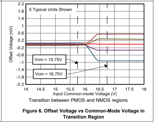
But latter, is shows 25uV is only the typical value, and only for PMOS, the offset of NMOS is more worse than that. I'm not very familiar with CMOS input OPs. So, any reason to specify the the Vos by MOS type? Which one should be used when designing.

Thanks.

  • Well you are looking at a RR input device - those often have crossover networks that operate near the positive supply - if you don't need RR input, then you can use the lower spec on this part or use a different part, here is a good discussion, 

    https://e2e.ti.com/blogs_/archives/b/thesignal/archive/2013/04/16/rail-to-rail-inputs-what-you-should-know

  • Hello Diverger,

    Michael's description and the lead he provided to the e2e blog by Bruce Trump should provide you with the explanation about the PMOS/NMOS input stage and how that design produces the somewhat different voltage offset across the OPA2156 input common-mode voltage range.

    The OPA2156 voltage offset vs. common-mode voltage (Vcm) is best visualized by the Typical Characteristics graph in the datasheet Figure 6.

    The PMOS differential pair is active from the negative Vcm limit to about +15.75 V. Between 15.75 V and 16.75 V both the PMOS and NMOS pairs are active to different extents. However, above about 16.75 V only the NMOS pair is on. Each input operating region will exhibit a somewhat different level of voltage offset. If the Vcm region is kept below about 15.75 V, the lowest offset voltage will be achieved as Michael suggested.

    Regards, Thomas

    Precision Amplifiers Applications Engineering