This thread has been locked.

If you have a related question, please click the "Ask a related question" button in the top right corner. The newly created question will be automatically linked to this question.

OPA2180: Rogowski coil signal acquisition

Part Number: OPA2180

      I now have a design that needs to collect the output signal of the Rogowski coil.The signal ratio of the coil is 1000A output  88mV, the rated input is 1000A, and can withstand 5 times overcurrent capability (ie 50000A). The signal from the Rogowski coil is amplified and integrated into the ADS8588S.The required accuracy is 0.5 grade accuracy, 5% or less is not required for accuracy, and 5% or more is required to be ±0.5%. The purpose is to obtain the current valid value, and there is no requirement for the phase.

I found a related reference design TIDA-00777 on the official website of TI. There are mainly the following problems.

1、Is there a need to divide the ciruit to two parts,One part is used for zooming in and the other part is used to integrate?

2、The op amp recommended by TIDA-00777 is OPA2188. Can  OPA2180 used in my previous project  be used to replace OPA2188. The price of both?

3、 Whether the ADS8588S acquisition range needs to be adjusted to ±5V to reduce the magnification?
4、 The structure of the circuit is that the input signal is first amplified, and then integrated. The amplification part is amplified in one step, and can be amplified by 100 times to ±4V(when the range of ADS8588S input is ±5V), or amplified by 200 times ±8V(when the range of ADS8588S input is ±10V), Or The amplification circuit amplifies a part,maybe 50 times, and the integration circuit enlarges a part,maybe 2 times. If you zoom in two levels, how to assign this amplification factor.
5、According to the TIDA-00777 circuit, the amplification part adopts in-phase amplification, and the integral adopts inverse integration. Do you have any better suggestions?
6、Is it necessary to add a protection device TVS tube in the place where the signal is input, and it is ok to use a 5V TVS tube. Still continue to use two 1N4148 parallel.

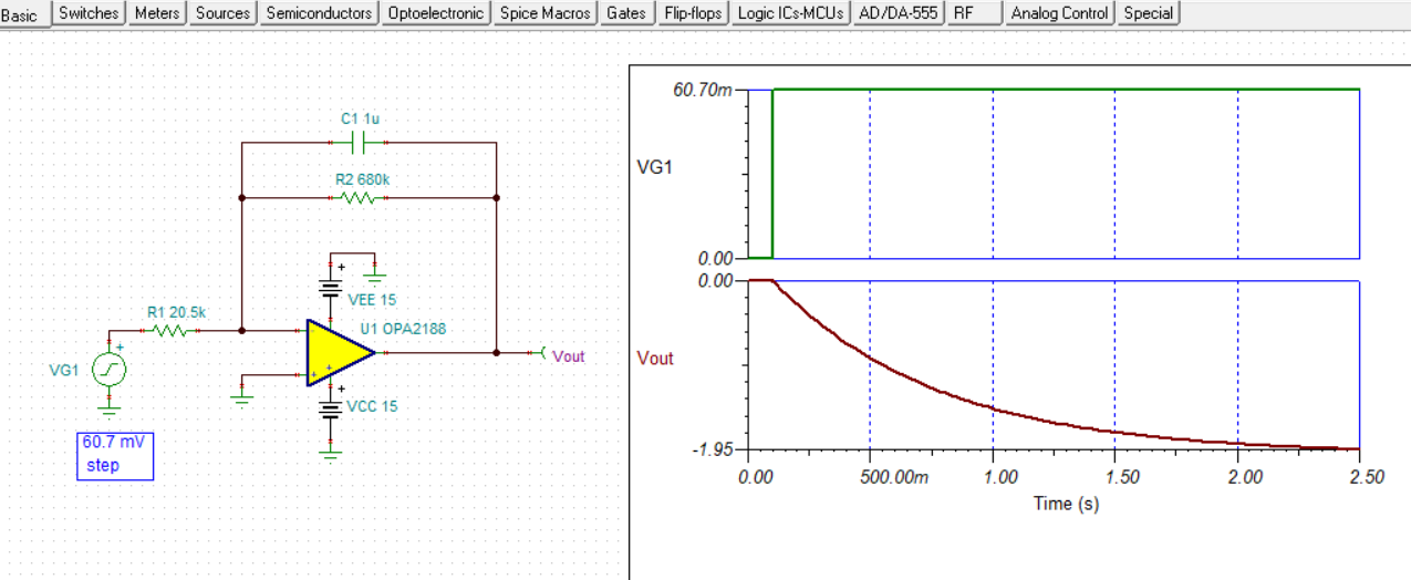
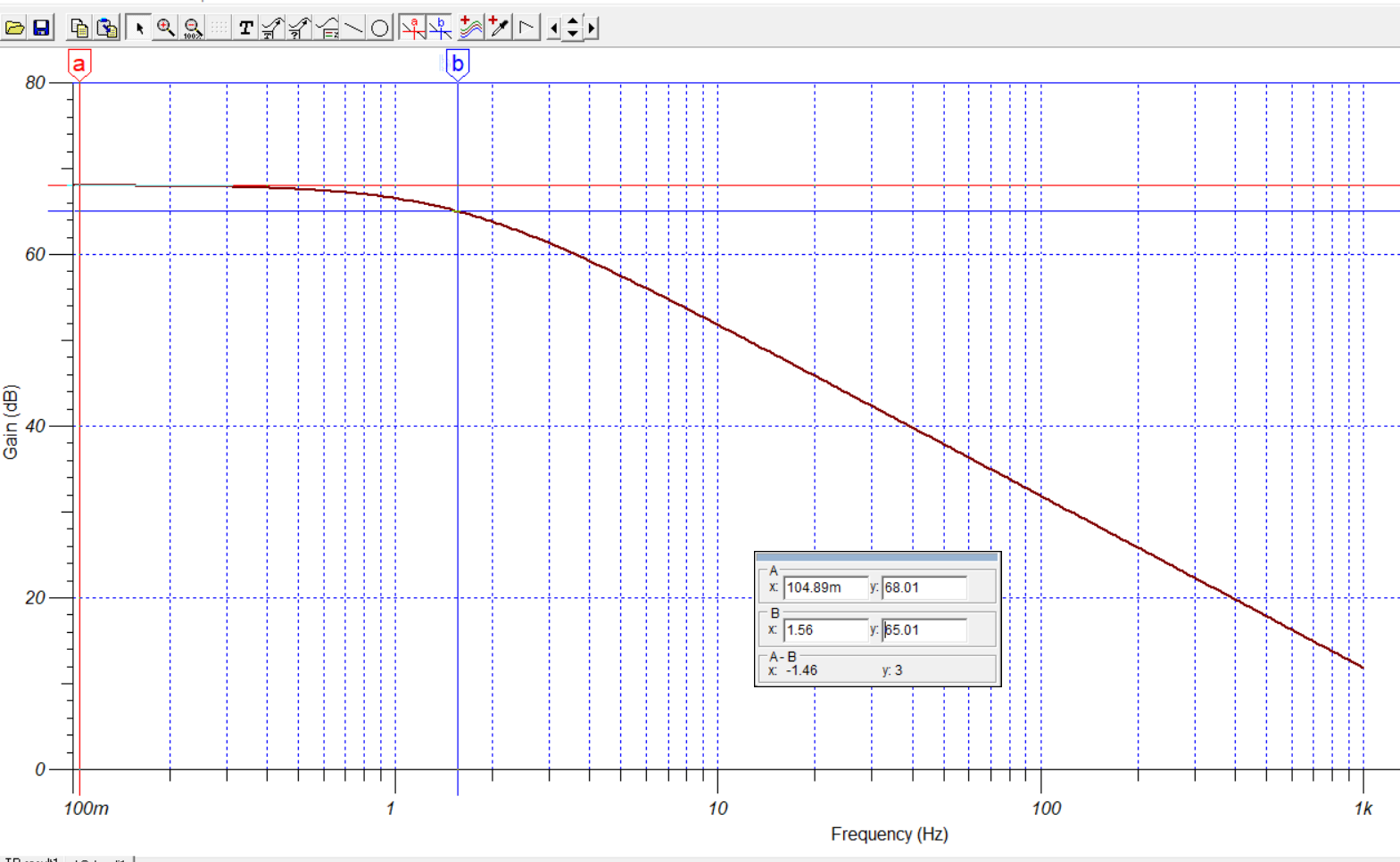
The above schematic is my design,The first level achieves 76 times magnification,The second level achieves 1.04 times magnification,Is there any problem with this design? Please give me some advice.

  • Hi user4973896,

    It does appear that the originators of this TI Precision Design included a good deal of information about the Rogowski coil input gain stage amplifier and integrator stage design considerations in the report. Since they optimized the design I do suggest that the information in the TI Design report be followed.

    1、Is there a need to divide the ciruit to two parts,One part is used for zooming in and the other part is used to integrate?

    The first stage following the Rogowski coil provides a 76 V/V voltage gain. For the 88 mV input (at 1000 Amps) the Op amp peak output voltage would be about 6.7 V. At much lower current levels such as 10 Amps the Op amp output will be down to about 60.7 mV. That should still be a usable level for the integrator that follows the first stage amplifier. If you need resolution down to even lower levels of output current, then you may want to consider a higher gain input stage.

    2、The op amp recommended by TIDA-00777 is OPA2188. Can  OPA2180 used in my previous project  be used to replace OPA2188. The price of both?

    Replacing the OPA2188 with the OPA2180 might result in a little higher voltage offset error. the OPA2188 is rated with a 25 uV max. offset (0.03 uV/C drift) and the OPA2180 is rated with a 75 uV max. offset (1 uV/C). The OPA2188 web page lists a $1.68/1 ku price. The OPA2180 we page lists a $1.26/1 ku price. I would certainly try the OPA2180 in the application and observe its performance and determine whether it is acceptable, or not.

    3、 Whether the ADS8588S acquisition range needs to be adjusted to ±5V to reduce the magnification?

    The ADS8588S is supported by TI's Converter Products group so they are most expert with the product. Reviewing the datasheet it states that the ADS8588S has pin-programmable bipolar inputs that can be set to ±10 V and ±5 V.


    4、 The structure of the circuit is that the input signal is first amplified, and then integrated. The amplification part is amplified in one step, and can be amplified by 100 times to ±4V(when the range of ADS8588S input is ±5V), or amplified by 200 times ±8V(when the range of ADS8588S input is ±10V), Or The amplification circuit amplifies a part,maybe 50 times, and the integration circuit enlarges a part,maybe 2 times. If you zoom in two levels, how to assign this amplification factor.

    The TI design can be optimized for either precision measurement, or fast settling. In Section 4.2.1.1 of the report for Precision Measurement the authors set the first stage gain to -16.3 V/V, and the integrator gain to -33.2 V/V, for an overall gain of 541 V/V. Then, in Section 4.2.1.2, Fast Settling, the set the first stage gain to -14.6 V/V and an integrator gain of -4.4 V/V, for an overall gain of 64 V/V; much lower gain. Your circuit with a gain of about 79 V/V is closer to the fast settling design.

    As indicated earlier for the 88 mV input the output from your design will be about 6.7 V peak. If the gain remains the same, then you would have to set the ADS8588S for the +/-10 V range. However, the gain amplifier circuit gain can be adjusted to accommodate either the +/-5 V, or +/-10 V ranges of the ADS8588S. You would need to look over the ADS8588S specifications and device which range provides the better performance relative to the application accuracy/speed requirements.


    5、According to the TIDA-00777 circuit, the amplification part adopts in-phase amplification, and the integral adopts inverse integration. Do you have any better suggestions?

    No.

    6、Is it necessary to add a protection device TVS tube in the place where the signal is input, and it is ok to use a 5V TVS tube. Still continue to use two 1N4148 parallel.

    If the fast, small-signal 1N4148 diodes are used as input clamps you should be able to apply the expected 88 mV input peak voltage without turning them on. If the input voltage does go into a 5x overload condition and assuming the Rogowski coil produces a linear response, about 440 mV peak would be present at the OPA2188/OPA2180 amplifier stage input. Likely, the 1N4188 diodes will just start conducting in the forward direction at that level and begin clamping the voltage to the forward bias level. Should the voltage increase beyond that the diodes will conduct all the more and clamp the voltage to some level below 800 or 900 mV. TVS diodes have intentionally higher breakdown voltage that will be volts, or higher. Therefore, with the 1N4148 input clamp diodes in place the TVS shouldn't turn on. You can add the 5 V TVS tube if you just want that extra margin of protection should one of the 1N4148 diodes open.

    Additionally, R9 is in series with the OPA2188 input and limits the current that could potentially flow into the amplifier ESD current paths. A resistance of almost 2 kilohm goes a long way in limiting the current.

    Regards, Thomas

    Precision Amplifiers Applications Engineering

  • 1. In the first answer ,60.7 mV is  still be a usable level for the integrator. Is there an available range limit for the input of the integrator?Why?

    2、I don't quite understand that the“ resistance of nearly 2 kiloohms has a long way to go to limit the current.”Does it mean that this resistance should be reduced?can i repace it with 0Ω。

    3、The capacitor of the integrator feedback loop uses a thin film capacitor, CAP, FILM, 0.15uF, 63VDC, 5%, RADIAL-2P,Can I replace it with a normal 0603 capacitor?if not ,WHY?

  • Hello user4973869,

    Regarding your questions:

    1. In the first answer ,60.7 mV is  still be a usable level for the integrator. Is there an available range limit for the input of the integrator? Why?

    TheOPA2188 integrator stage is completely usable with an input level of 60.7 mV, and a wide range of lower to  higher voltage levels as well. The constraint is the OPA2188 linear output voltage swing range on the high input voltage end. The linear output voltage range is specified as (V–) + 500 mV < VO < (V+) – 500 mV. Since the integrator stage in your schematic has a gain of -33.2 V/V the maximum input signal is limited to about +/-437 mV.

    On the low end of the usable input voltage range it comes down to the noise in the circuit as to how low of a signal level you can integrate. A complete noise analysis would have to be performed to determine the peak-to-peak input/output noise and just how large of input signal would be required to support a usable signal-to-noise ratio. You are probably looking at a minimum signal level in the millivolts on the low end.

    Below is an example of the OPA2188 integrating a +60.7 mV step input. Using a gain of -33.2 V/V, the maximum expected output voltage would be just about -2.0 V after about 5 time constants. You can see that it takes about 2.5 seconds for the integrator to produce an output close to the expected -2.0 V. The integration time is a function of the R2, C1 values selected for your circuit.


    2、I don't quite understand that the“ resistance of nearly 2 kiloohms has a long way to go to limit the current.”Does it mean that this resistance should be reduced?can i repace it with 0Ω。

    By virtue of the resistance being 2 kilohms a voltage applied at the input amplifier non-inverting input would have to be large for any appreciable current to flow. For example, if +10 V were applied at the input of R9 the maximum current that could flow would be +10 V/ 2 k would be 5 mA, which is under the OPA2188 maximum input current limit of 10 mA. In reality, about the only way that current level could be achieved with the resistor in place is if the ESD could somehow be turned on and the input current had a current path to flow through and return to ground. Leaving R9 out would provide no resistance to current flow and +10 V applied directly to the input would likely turn an ESD cell on and allow excessively high current to flow (>> 10 mA) and damage the Op amp input circuitry. 

    3、The capacitor of the integrator feedback loop uses a thin film capacitor, CAP, FILM, 0.15uF, 63VDC, 5%, RADIAL-2P,Can I replace it with a normal 0603 capacitor?if not ,WHY?

    The integrator capacitor quality matters in an integrator circuit. Low cost capacitors usually have a more lossy dielectric than that of a higher cost, film dielectric capacitor resulting in higher leakage current. That leakage current is an error current and you will find that the integrator output voltage can be different than that achieved by a capacitor having a high quality dielectric.

    A secondary issue with lower cost, non-film capacitors is the voltage coefficient characteristics which can become non-linear with increasing voltage across them. The film capacitor exhibits a much more linear voltage coefficient with applied voltage, which reduces another potential source of error in the integrator circuit.

    Regards, Thomas

    Precision Amplifiers Applications Engineering

  • 1、From the equation 3 in TIDA-00777 ,the gain of  Integrator is 1.04,why you say -33.2 which calculated only by 680k/20.5k.

    2、I understand that you mean a 2k resistor requires a large voltage to have any appreciable current as the ESD release path, so for me only 88mV, the highest is 440MV (88mv*5) input, I should  reduce this resistance to 88 ohms (0.44/0.005A), but you can't replace the resistor .Am I RIGHT?

  • Hello user4973896,

    1. If you apply Eq.3 from TIDA-00777, the integrator gain GAININV = (-RF || Xc)/R1. At low frequencies Xc is extremely high and can be dropped from the equation yielding -RF/R1. Using the two resistor values mentioned, GAININV = -RF / R1 = -680 k/20.5 k = -33.2 V/V. When the capacitive reactance is included it shunts the feedback resistance causing the impedance to drop and the resulting gain roll-off at higher frequencies.

    2. If the highest input voltage to the OPA2180 is 88 mV there is no need to include an over-voltage protection resistor. If you want to provide an extra measure of protection an 88 Ohm, or 100 Ohm resistor could be added.

    Regards, Thomas

    Precision Amplifiers Applications Engineering

  • 1、The capacitance inside the integrator is micro-level. As you said, in the case of 50hz, my overall amplification factor is not 76*1.04, it should be 76*33.2, which will far exceed the input of ADS8588S.

    2、Can you draw the ESD release path to me?

  • Hello user4973896,

    1. Yes, your circuit will have a much higher total voltage gain (2523 V/V) compared to the TIPD example.

    2. Have a look at Figure 43. "Equivalent Internal ESD Circuitry Relative to a Typical Circuit Application" in the OPA188 datasheet. The OPA180 uses the same internal ESD protection circuitry. Read through the Section 8.3.7 Electrical Overstress information. Keep in mind that the current associated with the EOS must have a path through the ESD circuitry back to ground. If you think of VIN as an EOS voltage the upper ESD diode connected between the +IN input and V+ is the most probable current path, but then that current has to have a return path to ground. If the EOS is a transient the power supply decoupling capacitor may provide an ac current path to ground. A sure solution is the TVS diode shown on each supply pin in Figure 43. A TVS diode will clamp an EOS event to a safe voltage and provide the current path back to ground.

    Regards, Thomas

    Precision Amplifiers Applications Engineering

  • So in the integral part of the op amp, if I want to achieve a gain of 1.04, and let the phase angle deviation be small, how to calculate.

  • So in the integral part of the op amp, if I want to achieve a gain of 1.04, and let the phase angle deviation be small, how to calculate.

  • Hello user4973896,

    The low frequency gain of the OPA2188 integrator stage is simply -RF/RI, or -R6/R11. If you want to maintain the same RC time constant, RF would need to be kept at 680 kilohms. Then, for a gain of -1.4 V/V, RI = 680 k/1.4 V/V, or 654 kilohms.

    The RF and RI values are very high resistances and contribute thermal noise. If these resistances can be reduced in value while maintaining the 1.04:1 ratio between them, the thermal noise can be reduced. An issue with doing this is that in order to maintain the same RC time constant C7 must be increased and can become large in value.

    If C7 is increased to 1 uF, a standard value, RF can be decreased to 102 kilohms and RI to 98 kilohms (1.04:1). The point that was made in an earlier response about the capacitor quality still applies, and a 1 uF film capacitor may become a size or cost limiting factor. If that is the case, then there is not choice but to use the higher value resistors.

    Regards, Thomas

    Precision Amplifiers

  • But when I simulated under the 50HZ low frequency, it didn't exceed 10V.The ratio is  not 2523 V/VTIDA-00777 - Gain + Integrator - Precision Measurement - 20190814.TSC

  • user4973896,

    The integrator has -3 dB cutoff frequency of:

    fc = 1/(2 pi RF CF) = 1 / (6.26 x 680 e3 x 150e-9) = 1.56 Hz

    Therefore, if you try pass a 50 Hz signal through the circuit the gain will be much reduced at that frequency. You can see a gain vs frequency simulation for the circuit.

    Regards, Thomas

    Precision Amplifiers Applications Engineering

  • From  the  gain vs frequency simulation for the circuit. i find the whole circuit gain is 37.83dB, so the gain RATIO is  76.03. So it is my problem. I didn’t tell you at the beginning that the input signal frequency of the Rogowski coil is 50HZ. Thank you very much for your patient explanation.Thank you very much!

  • Hello user4973896,

    I am glad to assist you with your precision amplifier application. If you now have all the information you need to move forward with your Rogowski coil application, it would be helpful if you could close this e2e inquiry.

    Should you need additional assistance down the road you can open a new e2e inquiry.

    Regards, Thomas

    Precision Amplifiers Applications Engineering