This thread has been locked.

If you have a related question, please click the "Ask a related question" button in the top right corner. The newly created question will be automatically linked to this question.

TLC2274: DC output voltage spike or distortion when coupled to MCU ADC

Part Number: TLC2274
Other Parts Discussed in Thread: OPA320, OPA197, OPA4197, OPA4191

Ref. Case CS0070966 (on TI support page) re-adressed to E2E

Original details: 

Spike or distortion of the DC voltage output of the OpAmp (used as DC voltage level shifter and 2nd order LPF) coupled to ADC input of MCU NXP MKV42F256VLH16 not programmed (standard condition for hardware pre-test before programming)

OPAmp STM TS914I and TS924I don’t shows any problem

Please find below  a detailed description of the problem with schematic and scope screenshots
We have our previous products in full production that uses this P/N since 2011
Now we are in components qualifying stage for a new product planned to replace the old ones

Problem Description

We encountered a problem coupling TI OpAmp TLC2274I to MCU NXP MKV42F256VLH16

Such OpAmp is used as DC voltage level shifter and 2nd order LPF (Butterworth non inverting topology), as represented in Fig. 1

OpAmp Output (signal V_ext) is connected to ADCB_CH0 input of MCU (pin 7) by a passive RC filter (R=1Kohm, C=100pF)

Critical working condition is test #4 of Tab. 1 below reported actually planned to be the standard test condition for hardware (pre-test before programming)

In the same application and test conditions alternative OPAmp STM TS914I and TS924I don’t shows any problem

Operating conditions of all test

Input voltage range of voltage level shifter:       Vext=±10Vdc

Output voltage range (OpAmp output):              V_ext=0÷3,3V

Analog power supply:                                                  Vcc=5,5V

ADC power supply:                                                       Vdda=3,3V

Digital power supply:                                                    Vdd=3,3V

All ICs have obviously its own Bypass Capacitors connected as near as possible to their Power Supply pins

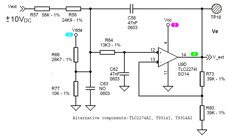
Fig. 1: Simplified electric diagram of DC voltage level shifter and 2nd order LPF

Test #

Test configuration

Vext applied

Test Result

NOTE

1

MCU not programmed, no other signal applied except Vext

-10 ÷ +10Vdc

PASS


2

MCU not programmed, signals applied as per Tab. 2 + Vext

-10 ÷ 0Vdc

PASS


3

MCU not programmed, signals applied as per Tab. 2 + Vext (same conditions of test #2)

0 ÷ 4,85Vdc

PASS?

Voltage spike on OpAmp output with amplitude depending by Vext voltage value applied

fig. 2 - CH4 (VEXT0003.png)

(@ Input voltage Vext=4,85V)

4

MCU not programmed, signals applied as per Tab. 2 + Vext (same conditions of test #2)

5 ÷ 10Vdc

FAIL

Distortion of the OpAmp

output with amplitude depending by Vext voltage value applied

fig. 3 - CH4 (VEXT0006.png) (@Input voltage Vext=9V)

5

MCU programmed, signals applied as per Tab. 1 + Vext

-10 ÷ +10Vdc

PASS


Tab. 1 schematic description of the problem encountered with TI Op amp TLC2274I

Signals applied to MCU ADC_CH0÷CH3 are obtained from other TLC2274I NOT contained in the case of D.U.T.

Vcc, Vdd, Vdda are not afflicted by voltages pulses or distortion (see. Fig. 3 and 4 CH2=Vcc and CH3=Vdda)

Voltage spikes and voltage distortion on OpAmp output are synchronous with AC signals applied to other ADC

(verified by triggering voltage spikes and modifying frequency of ADCA_CH0÷CH3 voltage applied)

Capacitor C63 is NOT assembled (test with 100nF had a negative result: C63 don’t solve the problem)

Signal name

MCU

pin

Average

DC component

Peak-to-Peak

AC component

Reference Image

ADCA_CH0_Vaux

5

+1,65V

1,34V

Fig. 2 - file MAVR3001.png

ADCA_CH1_VU

6

+1,65V

1V

ADCA_CH2_VV

9

+1,65V

1V

ADCA_CH3_VW

10

+1,65V

1V

Tab. 2: additional signals applied to MCU ADC_CH0÷CH3 test #2 ÷ #5

Fig. 2: additional signals applied to MCU ADC_CH0÷CH3 test #2 ÷ #5 - file MAVR3001.png

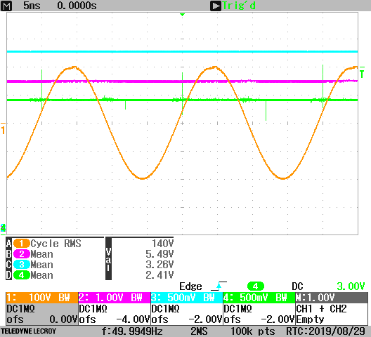
fig. 3 - Level Shifter Input voltage Vext=4,85V - file: VEXT0003.png - note voltage spikes on TLC2274 output (CH4)

fig. 3 -  Level Shifter Input voltage Vext=9V - file: VEXT0006.png - note output voltage distorsion on TLC2274 output (CH4)

As per information available on NXP MCU data sheet, in default mode pin 7 of MCU is configured as ADCB_CH0 input, its equivalent circuit cannot explain the problem described.

In conclusion the problem seems related to:

  • TI TLC2274I OpAmp
  • Unconfigured inputs of MCU NXP MKV42F256VLH16
  • AC signal applied to other  ADC channels (ADCA_CH0÷CH3)

Could you supply an explication?

Do you think there’s some solution rather than modify test procedure?

  • Hello Giovanni,

    Thank you for the very complete report of the performance you are observing with our TLC2274I Op amp. I suspect the output distortion that is occurring when the TLC2274I is applied is due its open-loop output impedance (Zo) characteristics and limited output current drive capability. Very likely, the MCU input acts upon the RC (1k, 100 pF) network and the TLC2274I output and demands different levels of current dependent on where it is at in its operating cycle. The transient current can be of a level that the circuitry preceding the MCU can't maintain the precise voltage level required for accurate circuit operation.

    The TLC2274I output current capability is in the single digit milliamperes range (see datasheet Figures 13 through 17), while the TS914/924 output capability is in the tens of milliamperes range (datasheet Figures 2 and 3). The graphs suggest the TS914/924 Op amp has much lower output impedance than the TLC2274I and it is capable of providing higher transient current when it required by the MCU input.

    The TLC2274I may not be the best choice for driving the RC network and MCU input because of its low output current drive. You may find that changing the R and C values in the network has some effect on the observed behavior. Decreasing the R and increasing the C may get bring the performance closer, or to what is needed.

    Alternately, there are other newer TI Op amps that would can provide higher current to the load. The high-voltage CMOS OPA197 and low -voltage OPA320 Op amps are suggested. Here are links to their web pages:

    http://www.ti.com/lit/ds/symlink/opa191.pdf

    http://www.ti.com/lit/ds/symlink/opa320.pdf

    The OPA320 is an especially strong A-to-D driver.

    Regards, Thomas

    Precision Amplifiers Applications Engineering

  • Hi, Thomas

    Thank you for the explanation and above all for the suggestions regarding alternative P/N.
    In order not to modify the PCB I will evaluate as possible alternatives OPA4191 and OPA4197, of which eventually I will ask for samples, also based on the logistical and economic evaluations I will receive from the Italian sales network.
    From the information available on the website it seems that the cost of the proposed components, even if budgetary, is decidedly higher than those used until now

    From the technical side, I have examined the data sheet graphs and at Vo=3.3V the maximum IOH current seems to be 2.95mA for the TI 2274 against 23.2mA of the TS914.
    However, it seems strange that the ADC channels of the MCU not programmed (configured by default as ADC) absorb current higher than 2.95mA and once programmed the MCU no longer have this anomalous absorption.
    I therefore asked for explanations also to NXP.

    BR

    Giovanni

  • Hello Giovanni,

    Do let us know if the OPA4191 and/or OPA4197 resolve the issue.

    Best regards, Thomas

    Precision Amplifiers Applications Engineering

  • Hello Giovanni,

    We hope your issue is resolved. I am going to close this thread now. Feel free to reply to to re-open if you have any questions moving forward.

    -Tamara

  • Hi Tamara,

    Formally the issue is't resolved, even if from the TI side the explication has been clear.

    I asked further information to NXP about the ADC ratings with MCU unprogrammed, I haven't got a definitive explication of the problem even it seems that really the unprogrammed MCU can sink more than 3mA on the ADC input.

    Nevertheless, as with the MCU programmed OpAmp works correctly, from a practical point of view the issue can be considered resolved: I changed the test procedure avoiding the critical working point

    With low priority, I will have further 2 test to perform:

    1) evaluate as possible alternatives OPA4191 and OPA4197, of which eventually I will ask for samples

    2) repeat the test in the critical condition BUT maintaining the MCU in RESET state

    In conclusion: my issue can be closed.

    Thanks for the support