This thread has been locked.

If you have a related question, please click the "Ask a related question" button in the top right corner. The newly created question will be automatically linked to this question.

OPA2990: Output Signal Distortion

Part Number: OPA2990

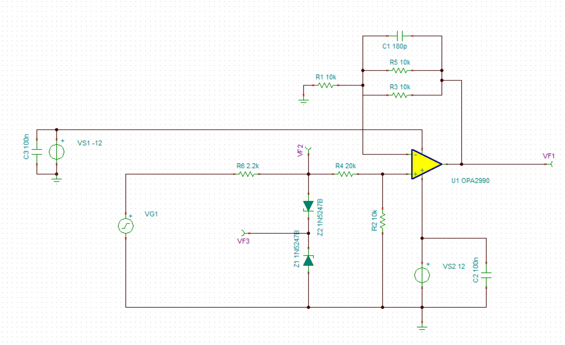
Hello TI community, recently I implemented the circuit attached below on a breadboard.

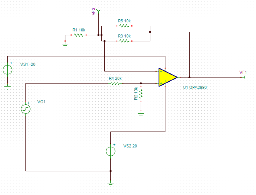
The ratio of attenuation looks good but when I tested the circuit with a sine wave as input the output shows distortion near of the peaks. This starts above 30 KHz and is evident with voltages above of 5 Vpp althought I have not done many tests varying the voltage of signal input. When frequencies below 30 KHz everything looks good even with high voltage swings, simulation in TINA were ok and based on the specifications of the OPAMP it should work ok but it does not besides the frequency of the signal is not so high for a breadboard and the configuration is high input impedance so the amplifier is not loading the input signal.

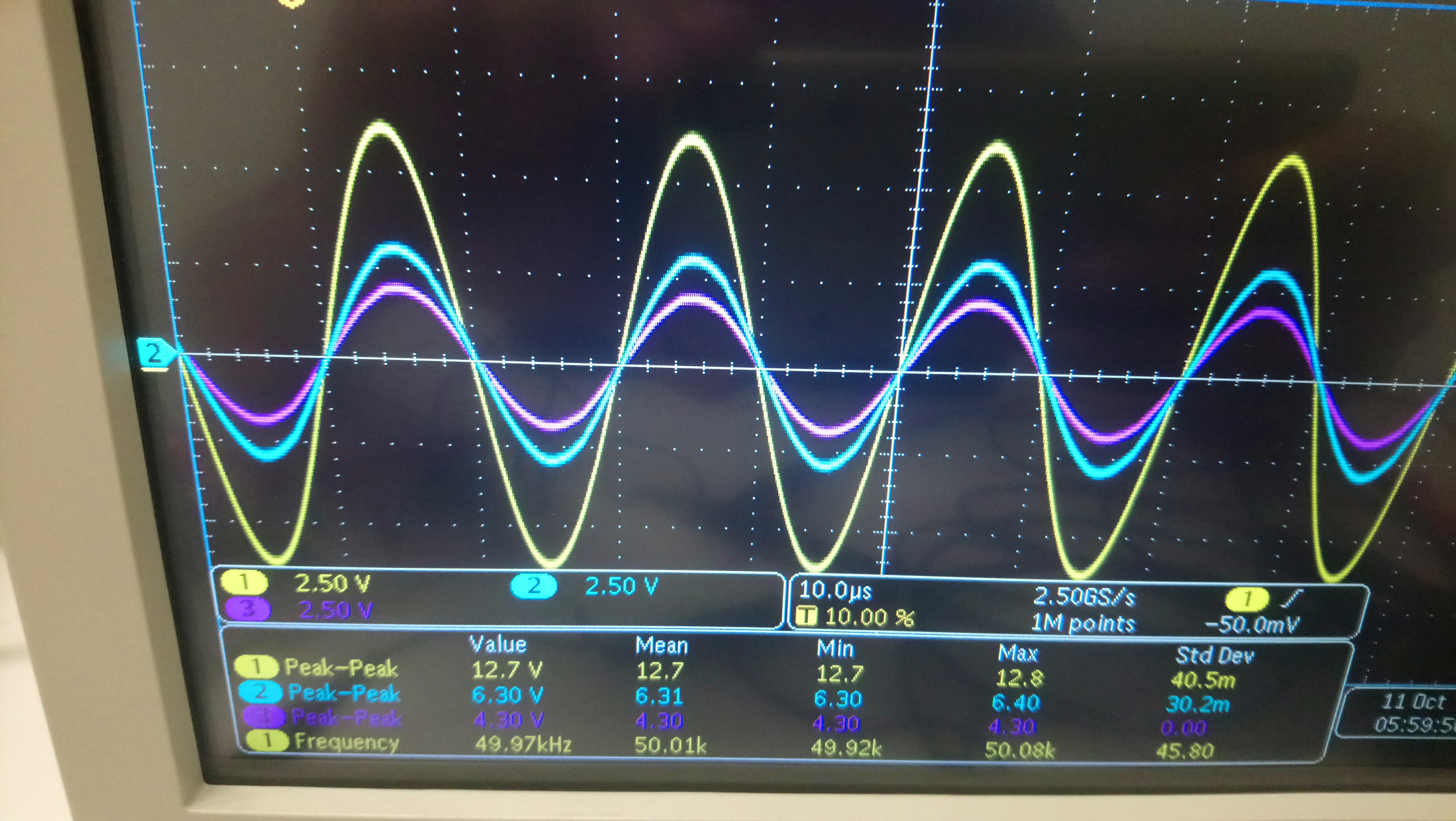
I will appreciate the help to figure out what is happening, if you need more information just tell me. Thanks in advance for the attention. 

  • Hi Andres,

    I believe the issue you are encountering is related to the slew rate of the amplifier. With a 6.3Vpp output the maximum input frequency must be less than ~113kHz to prevent going into slew induced distortion. Please see Figure 45 in the datasheet. I also recommend watching our TI Precision Lab Videos on Slew Rate.

    For frequencies less than 113kHz, the distortion you are seeing may be due to the slew boost feature turning on/off throughout the waveform.

    Thank you,

    Tim Claycomb

  • Hello Tim, thanks for your answer,  you are right, I have forgot the Slew Rate, actually the voltage swing that I want to achieve is 18 Vpp so my Max Freq will be around 40 KHz, the final goal of the circuit is the attenuation of signals with a fundamental frequency of max 1 KHz but the waveforms will be square waves.

    I was thinking about to add an active low pass filter to limit the bandwidth of the circuit and possible distortion using a 1 nF capacitor with the 5k resistor to establish a cut off frequency of 32 KHz, of this way I will get at least the first 20 harmonics and the shape of the square wave should be ok while I set the range of operation where the signals dont have distortion, what do you think?

    However for the second point: For frequencies less than 113kHz, the distortion you are seeing may be due to the slew boost feature turning on/off throughout the waveform. 

    How can I calculate or define the range where does the slew boost feature does not affect the circuit?  If you have a better part or other suggestions I will be happy to read them. 

    Thanks for the follow up of my question.

  • Hi Andres,

    I would put the low pass filter at the input of the circuit and would use a much faster OPAmp.

    Kai

  • Hi Andres,

    If the input signal is a square wave you shouldn't see the type distortion you are seeing with a sinewave. What you will see is the output signal rising or falling at a rate of approximately 4.5V/us. For an 18Vpp input the output will take approximately 4us to rise or fall to its final value. If my understanding of your system is correct I do not think you should need to filter the input signal unless you would like to reduce the total noise. Filtering will only slow down the transition from high to low or low to high.

    Thank you,

    Tim Claycomb

  • Hi Andres,

    It has been approximately one week since my last reply. Do you need any additional support?

    Thank you,

    Tim Claycomb

  • Hello Tim first of all thanks for the follow up and sorry for the delay since my last response: 

    I have changed the circuit to add additional protection, I will leave the cap of 180 pF as a placeholder just in case of I need it, you were right about that in my final case the main input waveform are square waves so the slew rate is involved at edges. I think that with sine waves the slew boost plays an important role so my output is different of my input even in low frequencies. 

    I wanted to provide a protection for the output to keep it between -10 to 10 VDC, I thought about back to back zener but I am including it on the input stage because of the parasitic capacitance however what would be your suggestion is it ok or should I moved it to the output part? About ESD, should I include some kind of protection or is ok with the built into the OPA2990, if no what would be your suggestion?

    Some time have happened since I made circuits and I am more a software guy but I would like to return HW Design and do this circuit of the best way. 

    Thanks in advance for your reply, the support of these forums is great.

  • Hi Andres,

    The output of the OPA2990 can still go to +/-12V should a fault, such as EOS (supply voltage spike, voltage spike on the output, etc.), occur to rail the amplifier. So if you want to protect anything connected to the output of the OPA2990 I would recommend adding clamping diodes to the output. If you do add diodes to the output make sure the capacitance of the diodes will not cause the phase margin to degrade below 45 degrees. I recommend watching our TI Precision Lab Videos on Op Amps Stability and EOS for more information.

    The ESD rating of the device are listed in table 6.2 on page 9 of the datasheet. The ESD ratings of the device meet industry standards. If you need additional protection, you would need to add components to slow down and reduce the current into the device. The document "2-wire, 4-20mA Transmitter, EMC/EMI Tested Reference Design" discusses some protection methods to improve the robustness of the design. The circuit is completely different than your design but I think the protection methods and ideas are still applicable.

    Thank you,

    Tim Claycomb