This thread has been locked.

If you have a related question, please click the "Ask a related question" button in the top right corner. The newly created question will be automatically linked to this question.

OPA356: Active Shield Driver for High(ish) Speed Capacitive Load

Part Number: OPA356
Other Parts Discussed in Thread: FDC2214, , LM79, LM7705, FDC2214EVM, FDC1004, OPA365

Hi,

I’m trying to design an active shield driver for the FDC2214 that is able to accurately voltage follow the half-sine, 10MHz, 3.6V signal.
The frequency can vary from 10kHz to 10MHz, and the amplitude can vary from 1.2V to 3.6V (not sure about the upper voltage limit).

The following image shows what I’m getting out of the oscilloscope but I think the peak is meant to be capped at 1.8V (I have an E2E thread open to resolve that. https://e2e.ti.com/support/sensors/f/1023/t/872784

Either way, it still gives a good idea of what shape the expected signal will take.

3.6V is the extreme I’m working with until I resolve the issues with FDC2214.

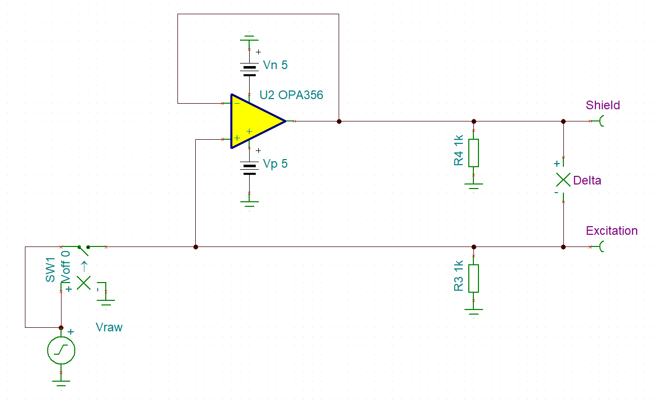
The minimum slew rate is 113.1V/µs (Slew rate = 2 π f V) but no op amp close to that value seems to work. I went for the overkill approach and drew up a simple schematic using OPA356 with a slew rate of 360V/µs, Gain Bandwidth Product of 200MHz and Small-Signal Bandwidth of 450MHz.

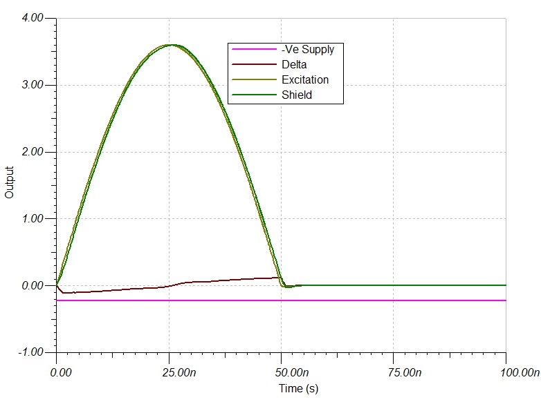
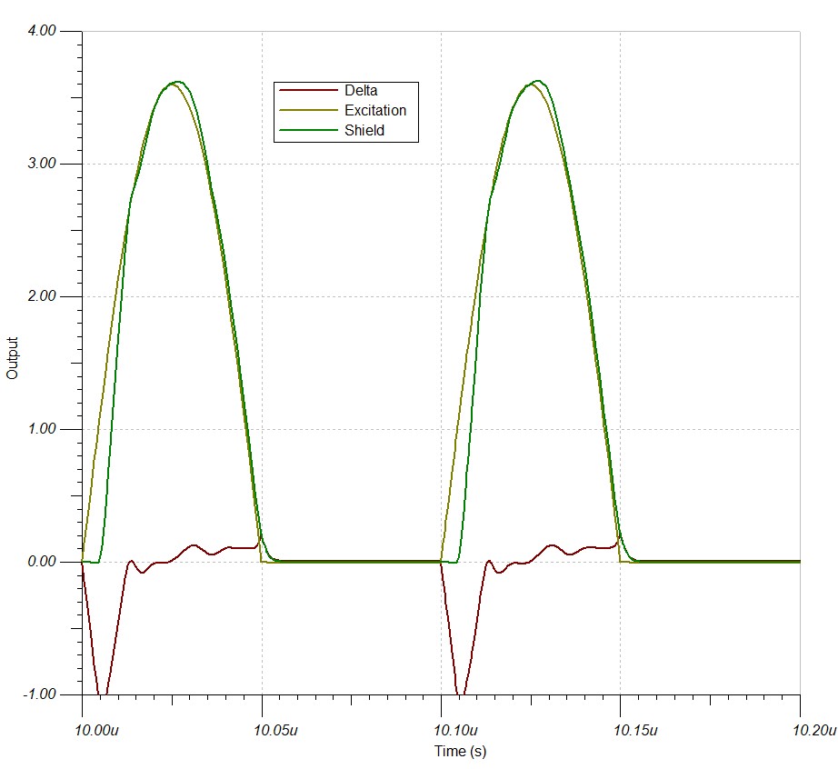
I can get the accuracy pretty close as can be seen in the simulations below. However, this simulation isn’t realistic due to the way I've set up the load.

In reality, the OPA356 will be driving a capacitive load which will be determined by the size of the sensor plates.

(1) How can we connect the OPA356 to drive a capacitive active shield?
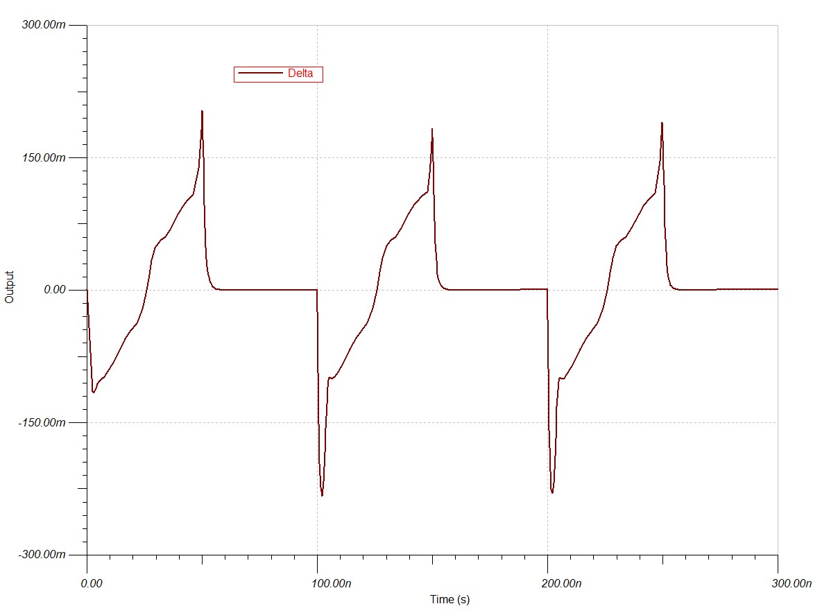
(2) Is it possible to improve the voltage tracking accuracy? In this simulation, we are looking at an inaccuracy of roughly -230mV to 200mV

(3) How do I setup the capacitive load in TINA TI?I’m not really sure what would accurately represent the capacitive plates. R3 and R4 definitely don’t represent the sensor layout but the simulation doesn’t work without them. I tried a few different passive configurations but they didn’t seem to work.

(4) Is there a better Op Amp that we could try?


Kind regards,

  • Hey Dan, 

    Interesting question, with good detail provided - before you get too far, recognize that no op amp actually goes to ground the output pin single supply, you might try the LM7905 to get a -0.23V negative supply (in sim first, just put negative supply to -0.23V). 

    Can you provide a TINA file to start with. 

  • Thanks Michael,

    The simulation file is attached at the bottom of this reply.

    I wondered about the 0V output. The OPA356 datasheet shows that he closest it should be able to get is 100mV but the simulation perfectly hits 0V. I just thought I hadn't set up the simulation correctly. Before moving to Tina TI, I was using LT Spice which clearly showed the lower offset. Setting the OPA356 negative supply to -0.3V didn't change anything in the simulation since it was already showing 0V in the space where the input signal was 0V. It also didn't change the part of the wave where the largest difference was.

    If we absolutely have to include a negative supply, we will. But we definitely want to explore other options first. Unless there is a very efficient and low quiescent way of achieving it.
    The issue is that this product needs to be able to hibernate on battery for a very long time (we're targeting years) and the FDC2214, and therefore the shield driving op amp, is one of the few components that will be active during hibernation so power consumption is a big factor.
    That's another reason why I asked if there's an alternative op amp since the OPA356 is relatively hungry in comparison to some others. Although I'm hoping that rail to rail, high slew, high bandwidth, capacitive load and low current consumption isn't too much to ask; but I'm aware that it might be. I'm aiming to get as close as possible.

    Tina TI Simulation

    Shield (Tina TI).TSC

    The OPA356 spice mode is from the TI website (http://www.ti.com/lit/zip/sbom849

    Kind regards,

  • I just realised that I forgot to change the op amp to LM7905 when I added the negative supply. Sorry I'll do that as soon as I get back to the office. Hopefully tomorrow morning.

  • No, the LM7905 is a regulator to get that -0.23V supply, stay with the OPA356 for now, 

  • Thanks Michael,

    I couldn't find LM7905 (or LM79) in Tina TI and the model isn't available to be downloaded from the TI website. http://www.ti.com/product/LM79

    Instead, I added a generic 5V supply with the positive grounded and the negative on the negative supply of the OPA356 to create a -5V. Just for simulation purposes since ±5V exceeds the input range of the OPA356.

    Would that be enough for this test? If not, I'll keep looking for the LM7905. The measurement showed that it was working as a negative supply in simulation, even if it was an ideal supply.

    The result was as follows. The difference (labelled as Delta) between the excitation signal (input) and the shield signal (output) was reduced. I'm not sure why because the error should be in the second half of the wave (50ns - 100ns) where both signals are 0V. I do want the 0V, or as close as possible, but shouldn't the OPA356 have 100mV on the output during this section? The first half of the wave (0ns - 50ns) is affected by slew and bandwidth which didn't change.

    The Delta between both signals with 0V on the negative supply of the OPA356 is also slightly different to what I posted yesterday with the only difference being the computer that I ran the simulation on. The second computer is a more powerful machine; is that difference normal for Tina TI?

    OPA356 with 0V on the Negative Supply


    OPA356 with -5V on the Negative Supply

    Kind regards,

  • Oops, I meant to say LM7705 negative fixed voltage regulator, no TINA model apparently, but just put -0.23V on the negative supply pin of the op amp, 

    http://www.ti.com/lit/ds/symlink/lm7705.pdf

  • A negative supply of 0V and -5V are in a previous comment above.

    A negative supply of -0.23V is below, including an extra measurement in the plots for verification.

    OPA356 with -0.23V on the Negative Supply

    Kind regards,

  • Morning Dan, 

    I was stepping through this closer, must admit to be pretty confused by your situation. Are you really trying to create a 1/2 sine wave by clipping the single supply op amp into ground. Sim models do a very poor job of reporting that in detail.  The source is bipolar apparently, but is that the real source. And what is your real load. 

    You are describing this as a shield driver which is kind of odd, not sure what you mean by that and is that not really a capacitive load. 

    In any case, if you really have a 10Mhz 1/2 sinusoid signal - 

    1. probably need at least 100Mhz BW 

    2. Your power concerns? Can't you use a disable part that goes to very low power in your offstate? 

  • Thanks Michael,

    Shield

    The device generating the half sine excitation signal is a TI FDC2214. "INA is excited with a half sine wave and INB is excited with the same half sine wave shifted by 180 degrees." - Rachel Liao, Texas Instruments, https://e2e.ti.com/support/sensors/f/1023/t/536824?FDC2214-how-to-excite-LC-tank

    In the measurement below (from the FDC2214EVM dev kit), the frequency is 4.75MHz, but the FDC2214 is capable of exciting at 10KHz through to 10MHz. We don't know which frequency will best detect our material so during prototyping we would like to be able to test any frequency within the FDC2214 range.

    As you can see, the steady state maximum voltage is roughly 1.8V but the transient exceeds this at roughly 2.5V.

    The FDC1004 has a built in shield driver, but excites at a fixed frequency that we need to avoid. The FDC2214 is perfect since we can control the frequency; however, it doesn't have a built in shield driver. I need to create one using an op amp, and configure it so that it can drive the capacitive load.

    Our sensor is configured in a similar way to the image below. We have:

    • a sensor plate with the excitation frequency,
    • a second plate that will be either grounded or connected to a differential sensor plate (we will test both),
    • a shield plate behind (as well as a guard ring if necessary).

    The shield signal must as close as possible equal the excitation frequency to eliminate any potential between them. This is why we are trying to drive it through a voltage following op-amp using the excitation frequency as an input.

    Simulation

    Source

    I'm new to Tina TI and didn't know how to configure the source to match the half sine shown in the oscilloscope image above so I used a full wave sinusoidal voltage generator and an ideal voltage controlled switch with a 0V trigger. I'm used to LT Spice.

    Load

    This might be a better representation of the load in the Tina TI simulation.

    OPA356 with 0V on the Negative Supply

    OPA356 with -0.23V on the Negative Supply

    Low Power Consumption

    This sensor will be on all the time. This was something to consider if there is a better alternative to the OPA356.

    Op Amp Specifications

    I found the OPA356 by searching for ≥ 200V/µs slew and ≥ 200MHz bandwidth

    The Problem

    1. I need to find a way for the OPA356 (or alternative if you know of one) to drive the capacitive load without it becoming unstable.

    2. I need to find a way to help the op amp follow the excitation frequency as closely as possible to reduce the potential between the shield and the excitation signal. I need to consider power consumption which probably means avoiding a negative supply, but only if possible.

    An attempt

    The OPA365 (different device) datasheet gives a brief explanation of how to drive a capacitive load and output (close to) 0V on a single supply (page 12 and 13). The device itself is far too slow but I tried to apply this information to the OPA356. It seemed to make things worse at 3.6Vpk, and even worse at 1.8Vpk.

    Attachments

    Shield (Tina TI) 2.TSC


    Kind regards,

  • Thanks Dan for the detail, 

    Actually a tough problem, but I do wonder if the FDC part can actually generate that clean of a signal into a 100pF load - assuming it can, here is some discussion, 

    half wave Cload driver with OPA356.docx