Other Parts Discussed in Thread: TL081, TMCS1100, TLV2461
8.3.1.2 Input Signal Bandwidth
The INA240 input signal, which represents the current being measured, is accurately measured with minimal disturbance from large ΔV/Δt common-mode transients as previously described. For PWM signals typically associated with motors, solenoids, and other switching applications, the current being monitored varies at a significantly slower rate than the faster PWM frequency. The INA240 bandwidth is defined by the –3-dB bandwidth of the current-sense amplifier inside the device; see the Electrical Characteristics table. The device bandwidth provides fast throughput and fast response required for the rapid detection and processing of over current events. Without the higher bandwidth, protection circuitry may not have adequate response time and damage may occur to the monitored application or circuit.
Q1: What technical Wiki leads datasheet to making (blue) and seemingly false narrative statement?
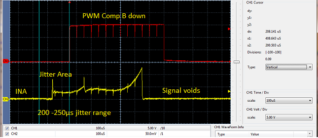
If that were entirely true then synchronous triggered ADC samples derived from PWM driven inductive events would be mostly seen as asynchronous to the hardware creating the events.
Q2: Could it be the limited band width (400KHz) has lead to an mostly incorrect deduction due to INA phase shifting of output events partially occurring outside typical ADC sample window?
It would seem INA shunt calculator error % increases exponentially due to slower asynchronous current events if or when hardware attempts samples via a synchronous windows.
Q3: What modification to INA can be made to keep the output synchronous with PWM frequency events timing?