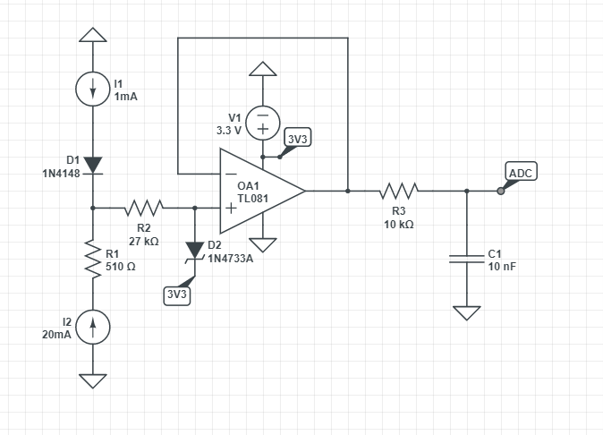
This thread has been locked.

If you have a related question, please click the "Ask a related question" button in the top right corner. The newly created question will be automatically linked to this question.

TLV9051: TLV9051 Clamp Diode with External One

Part Number: TLV9051

Hi, everyone,

We need to protect the resistor input using TLV9051 against the wrong connection such as 4-20mA current input.

I know the voltage will never reach 20mA thanks to series resistance.

Since connecting the output of it to ADC input directly, VCC voltage must be 3.3V and VEE 0V.

TLV9051 has an internal clamp diode. If connecting an external Schottky diode for clamping to 3.3V which one makes clamp, internal or external?

  • Former Member
    0 Former Member

    Hello Gokhan,

    Can you please clarify, what is meant by "the wrong connection such as 4-20mA current input."  Where would this current come from?  Is it shown in the schematic above?

    Also, you say "I know the voltage will never reach 20mA thanks to series resistance."  Do you mean the current into the input pin of the amplifier will never reach 20mA?

    I'm not sure I understand the proposed current path through your circuit.  It would seem that the 1mA source current would go through the D1 diode and then through R2.  Similarly, the I2 current would go through R1 and then R2.  So, you would potentially have up to 21 mA seeking to enter the input of the amplifier, as shown below.  Is this desired, or is it the "wrong connection" you are trying to protect against?

    As for your question, I think the external D2 Schottky diode would turn on first.  If you look in section 7.1 of the TLV9051 datasheet, you will see that the absolute maximum common-mode input voltage is 500 mV beyond the rail.  The schottky diode typically has a lower forward voltage drop.  So if your VCC is 3.3V, for example, then the internal diodes will conduct when the input voltage reaches ~3.8V.  However, the Schottky diode will start to conduct earlier possibly between ~3.5V and ~3.7V.

    Finally, if you still need help selecting components for R3 and C1, I recommend you download our Analog Engineer's Calculator.  There is a section under "Data Converters" called "ADC SAR Drive" which can help you select component values for your low-pass filter.

    Regards,

    Daniel Miller

  • Hi Gokhan,

    I don't have any idea about what you want to say. And I don't see the TLV9051 in your schematic either. And what is the purpose of the zener diode D2 in your circuit?

    Kai

  • Former Member
    0 Former Member in reply to kai klaas69

    Hello Gokhan,

    Kai brings up a good point.

    When you mentioned the "Schottky diode," I assumed you were referencing D2.  But looking at it more closely, it looks like D2 is actually a Zener diode in your schematic.

    Can you please clarify which diode you are referring to?

    Thank you,

    Daniel

  • Former Member
    0 Former Member in reply to Former Member

    Hello Gokhan,

    We have not heard back from you in a while.  Do you still need help?

    If so, please let us know.  Otherwise, I will assume that you've found a resolution and will close this thread.

    Regards,

    Daniel

  • Thank you. I designed it with Schottky for input. I knew the clamp diode was active when it reached VCC, I was wrong.

  • Hi Gokhan,

    do you still need help? You might want to show your latest schematic?

    Kai